PCB-based current detection device

A current detection device, PCB board technology, applied in the direction of measuring devices, measuring current/voltage, measuring electrical variables, etc., can solve the problem of weak ability to resist external magnetic field interference, and achieve strong anti-external magnetic field interference and strong ability Effect

Pending Publication Date: 2019-05-14
NING BO SINOMAGS ELECTRONICS TECH CO LTD
View PDF0 Cites 1 Cited by
  • Summary
  • Abstract
  • Description
  • Claims
  • Application Information

AI Technical Summary

Problems solved by technology

[0005] In view of this, the embodiment of the present invention provides a PCB-based current detection device

Method used


Image

  • PCB-based current detection device
  • PCB-based current detection device
  • PCB-based current detection device

Examples


Embodiment 1

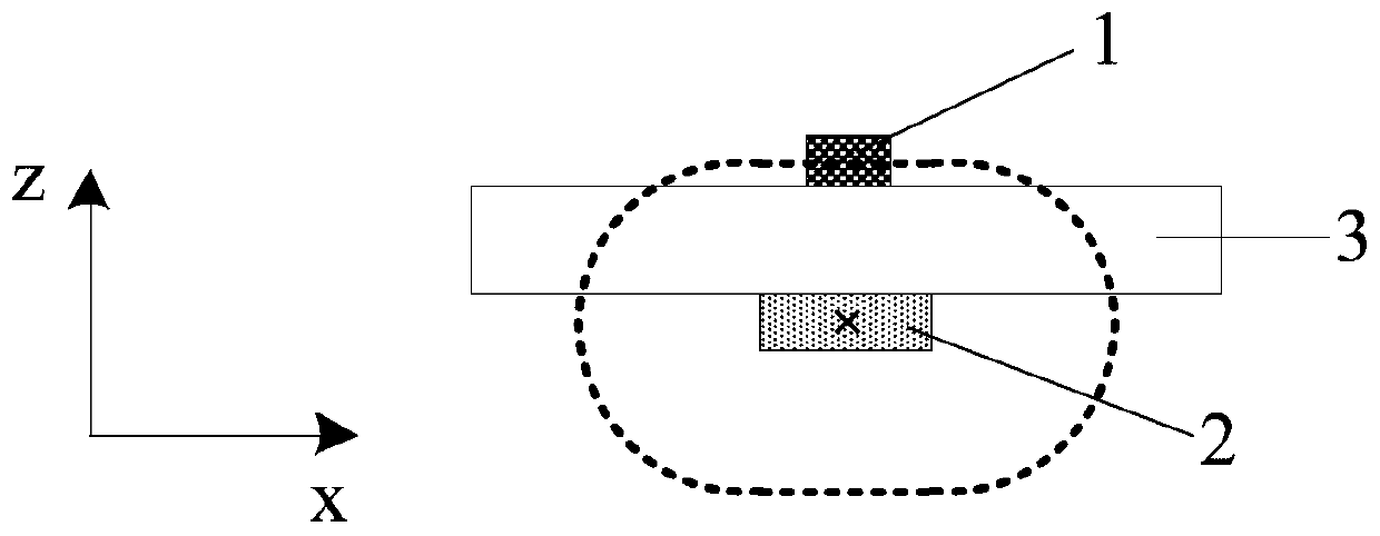
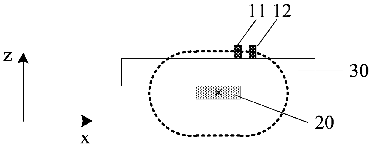
[0037] An embodiment of the present invention provides a PCB-based current detection device, Figure 2A shows its side view, Figure 2B A schematic diagram of its overall structure is shown, Figure 2C shows its top view, where, Figure 2A The "×" in the wire 20 indicates the direction of the current flowing in the wire (that is, from one side of the paper or screen where the reader is located to the other side), Figure 2B and Figure 2C The arrow inside the middle wire 20 and Figure 2A Corresponding to the "×" in the wire, it is also used to indicate the direction of the current flowing in the wire. The device comprises a first magnetoresistance 11, a second magnetoresistance 12, a wire 20, a PCB body 30 and a signal processing module ( Figure 2A , Figure 2B and Figure 2C not shown).

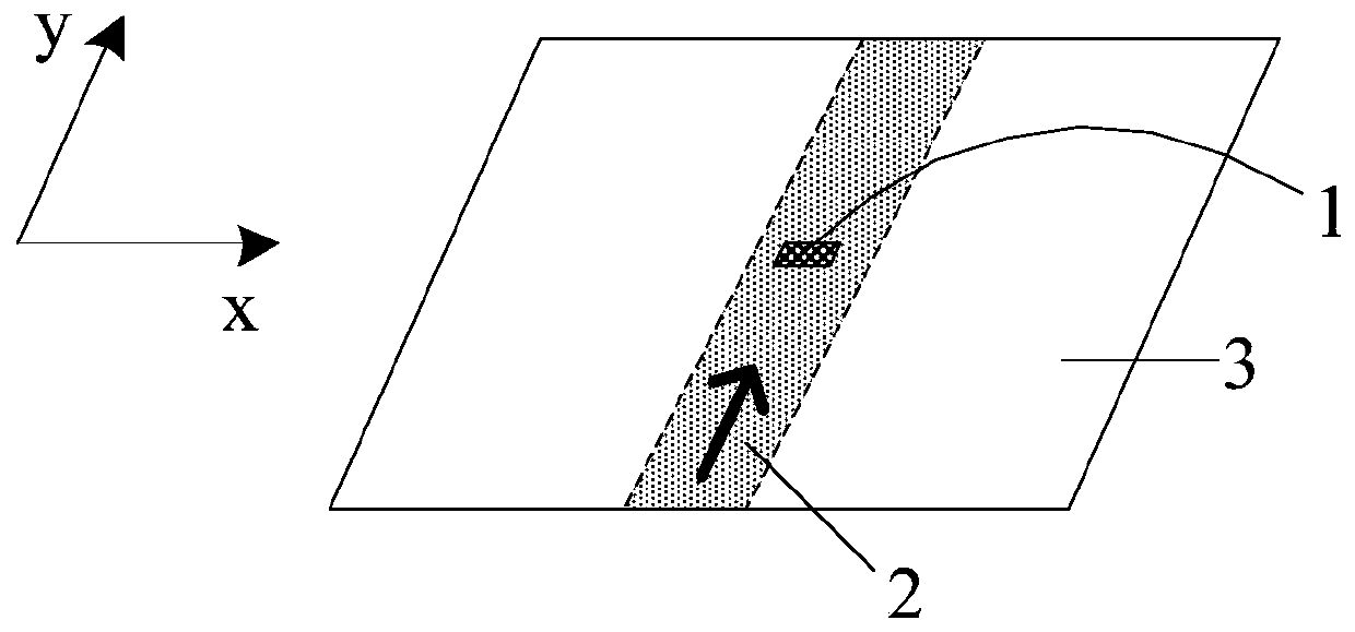
[0038] The wire 20 is printed on the first surface of the PCB body 30 for passing the current to be measured. Both the first magnetic resistor 11 and the second magnetic resistor ...

Embodiment 2

[0050] The embodiment of the present invention provides another PCB-based current detection device, Figure 5A shows its side view, Figure 5B A schematic diagram of its overall structure is shown, Figure 5C Its top view is shown. control Figure 2A to Figure 2C It can be seen that the difference between the device provided by the embodiment of the present invention and the first embodiment is that the device includes four magnetoresistances, that is, the first magnetoresistance 11, the second magnetoresistance 12, the third magnetoresistance 13 and the fourth magnetoresistance resistor 14 instead of two magnetoresistors. The specific arrangement of the four magnetoresistances in this embodiment will be described in detail below.

[0051] Such as Figure 5A As shown, the wire 20 used to pass the current to be measured is printed on the first surface of the PCB body 30, and the first magnetoresistance 11, the second magnetoresistance 12, the third magnetoresistance 13, an...

Embodiment 3

[0059] The embodiment of the present invention provides another PCB-based current detection device, the only difference between it and the second embodiment is that the magnetic sensitivity directions of the four magnetoresistors are the same.

[0060] Such as Figure 6 As shown, the first branch where the first magnetoresistance 11 and the second magnetoresistance 12 are located can be regarded as image 3 In the circuit shown, the second branch where the third magnetoresistance 13 and the fourth magnetoresistance 14 are located can also be regarded as image 3 circuit shown. Because the magnetic induction at the position of the first magnetic resistance 11 is greater than the magnetic induction at the position of the second magnetic resistance 12, the magnetic induction at the position of the fourth magnetic resistance 14 is greater than the magnetic induction at the position of the third magnetic resistance 13, and also That is, when placed in a magnetic field environment...


PUM


Abstract

The invention discloses a PCB-based current detection device, wherein the device comprises a PCB body, a conducting wire, a first magnetic resistor, a second magnetic resistor and a signal processingmodule; the conducting wire is printed on the first surface of the PCB body, and used for introducing current to be detected; the first magnetic resistor and the second magnetic resistor are arrangedon the second surface of the PCB body; the second surface is opposite to the first surface; the distances of the first magnetic resistor and the second magnetic resistor between projection in a plane,where the conducting wire is, and the conducting wire are different; both the magnetic sensitive directions of the first magnetic resistor and the second magnetic resistor are parallel to the PCB body; furthermore, the magnetic sensitive directions of the two are same; the first magnetic resistor and the second magnetic resistor are connected in series; the two ends, which are connected in series, are connected to a power supply; and the input end of the signal processing module is connected between the first magnetic resistor and the second magnetic resistor, and used for obtaining an outputto-be-detected current value according to an electric signal between the first magnetic resistor and the second magnetic resistor. The external magnetic interference resistant capability of the PCB-based current detection device provided by the invention is relatively high.

Description

technical field [0001] The invention relates to the technical field of current sensors, in particular to a PCB-based current detection device. Background technique [0002] Current detection products are widely used in new energy, intelligent transportation, industrial control, smart home appliances and smart grid and other fields. Current detection products are usually packaged chips. At least two pins of the chip are used to introduce or lead out the current to be measured. These two pins are also connected by wires inside the current detection chip; they are actually used to sense the magnetic field to realize The magnetic sensor with the function of detecting current is also packaged in the chip, and the magnetic sensor is close to the wire connecting the above two pins. This current detection chip has the following disadvantages: (1) the withstand voltage of the chip is low; (2) the cross-sectional area of ​​the above-mentioned wire connecting the two pins is small so ...

Claims


Application Information

Patent Timeline
IPC IPC(8): G01R19/00
Inventor 朱海华王建国白建民于方艳
Owner NING BO SINOMAGS ELECTRONICS TECH CO LTD
Why Eureka
Try Eureka