Bonding structures and methods of forming them

A technology of bonding structure and scheme, which is applied in the direction of semiconductor/solid-state device parts, semiconductor devices, electrical components, etc., can solve problems such as increased cost, decreased product reliability, and shortened electromigration life, so as to improve reliability and avoid Reliability deterioration, avoiding the effect of electrical performance degradation

Active Publication Date: 2021-02-23
YANGTZE MEMORY TECH CO LTD
View PDF6 Cites 0 Cited by
  • Summary
  • Abstract
  • Description
  • Claims
  • Application Information

AI Technical Summary

Problems solved by technology

[0004] However, in the prior art, at the bonding surface of the metal interconnection between the memory array structure and the CMOS circuit structure, metal atoms are prone to diffusion and electromigration during the heating and cooling process of the bonding process and after bonding, so that the metal bond Pores are generated in the joint surface, resulting in leakage, shortened electromigration life, etc., which reduces the reliability of the product
In the prior art, in order to reduce the above problems, many adjustments and reliability control of the chemical mechanical polishing process for forming metal interconnections are required, resulting in increased costs

Method used


Image

  • Bonding structures and methods of forming them
  • Bonding structures and methods of forming them
  • Bonding structures and methods of forming them

Examples


Embodiment Construction

[0026] The specific implementation of the bonding structure provided by the present invention and its forming method will be described in detail below in conjunction with the accompanying drawings.

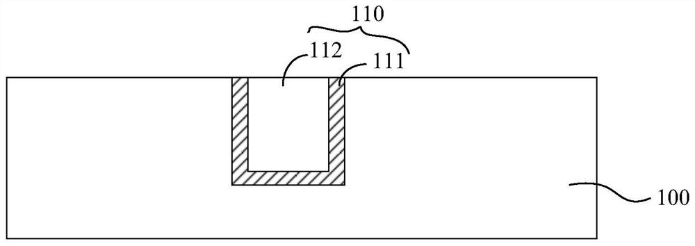
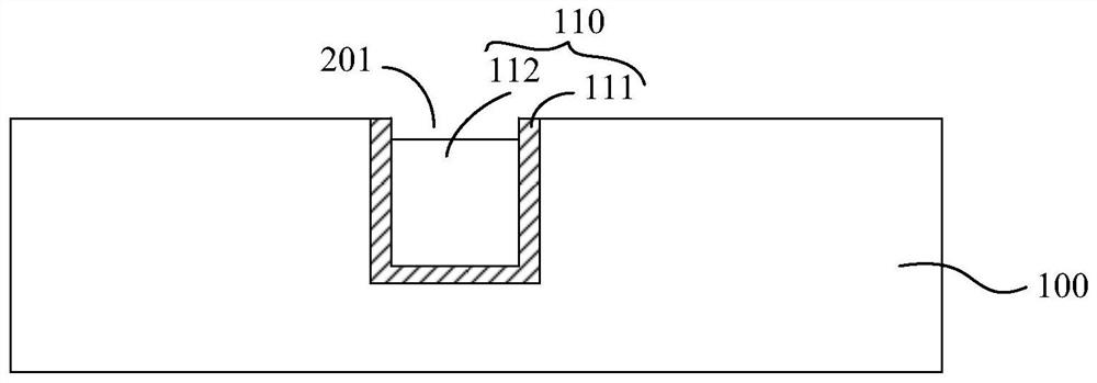
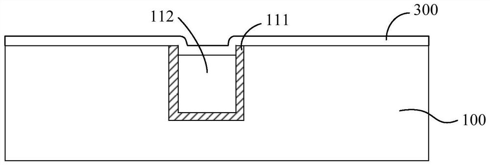
[0027] In a specific embodiment of the present invention, the method for forming the bonding structure includes: providing two substrates, each of which includes a dielectric layer and a metal interconnection on the exposed top surface within the dielectric layer; The barrier layer is formed on the surface of the metal interconnection at the opposing bonding position of the substrates, and when the metal interconnecting portions are provided at the opposing bonding positions of the two substrates, at least the top surface of the metal interconnecting portion with a larger size is formed. A barrier layer, the barrier layer is a conductive material and can block the diffusion of metal atoms; the surfaces of the two substrates are bonded to each other, and the barrier layer is located...


PUM

PropertyMeasurementUnit
thicknessaaaaaaaaaa
thicknessaaaaaaaaaa

Abstract

The present invention relates to a bonding structure and a method for forming the same, comprising: providing two substrates, each of which includes a dielectric layer and a metal interconnection formed in the dielectric layer with an exposed top surface; The surface of the metal interconnection at the bonding position forms a barrier layer, and when the two substrates are provided with a metal interconnection at the opposing bonding position, at least a barrier layer is formed on the top surface of the larger-sized metal interconnection. , the barrier layer is a conductive material and can block the diffusion of metal atoms; the surfaces of the two substrates are bonded oppositely, and the barrier layer is located between the metal interconnections of the two substrates. The barrier layer can prevent the metal atoms in the metal interconnection from diffusing to the adjacent dielectric layer, avoid the electrical performance and reliability deterioration of the device caused by the metal atom diffusion, and improve the reliability of the bonded device.

Description

technical field [0001] The invention relates to the technical field of semiconductors, in particular to a bonding structure and a forming method thereof. Background technique [0002] In recent years, the development of flash memory (Flash Memory) is particularly rapid. The main feature of flash memory is that it can keep stored information for a long time without power on, and has the advantages of high integration, fast access speed, easy erasing and rewriting, etc. Has been widely used. In order to further increase the bit density (Bit Density) of the flash memory while reducing the bit cost (Bit Cost), three-dimensional flash memory (3D NAND) technology has been developed rapidly. [0003] The 3D NAND flash memory structure includes a memory array structure and a CMOS circuit structure above the memory array structure. The memory array junction and the CMOS circuit structure are usually formed on two different wafers, and then bonded to The CMOS circuit wafer and the ...

Claims


Application Information

Patent Timeline
Patent Type & Authority Patents(China)
IPC IPC(8): H01L21/60H01L23/538H01L27/11524H01L27/11551H01L27/1157H01L27/11578
CPCH01L2224/08145
Inventor 王先彬肖莉红李涌伟
Owner YANGTZE MEMORY TECH CO LTD
Why Eureka
Try Eureka