Manufacturing method of light-emitting diode micro-crystal grains

A technology of light-emitting diodes and manufacturing methods, which is applied in the direction of electrical components, circuits, semiconductor devices, etc., and can solve the problems of not deep ablation of grains, difficulty in peeling off good-quality grains from semiconductor substrates, and excessive ablation

Inactive Publication Date: 2019-05-14
ZHANJING TECH SHENZHEN +1
View PDF4 Cites 0 Cited by
  • Summary
  • Abstract
  • Description
  • Claims
  • Application Information

AI Technical Summary

Problems solved by technology

[0003] In the prior art, before the good product die / chip is separated from the semiconductor substrate, it is necessary to ablate the bad die on the substrate (laser ablation). Due to the control and uniformity of the laser power, the die / chip The etching efficiency of the epitaxial layer is different, which will cause the problem that the grain ablation is not deep and remains or the grain ablation is too deep
In the flip chip process, an auxiliary substrate is used to assist the separation of the die, that is, the substrate formed with an adhesive layer is pressed on the surface of the die, and the laser is used to irradiate the semiconductor substrate, so that the laser will pass through When the semiconductor substrate reaches the adhesive layer, the position where the laser beam reaches the residual grain, the position where the ablation is too deep, and the gap between the good product grains; the adhesive layer is coked due to the laser energy, causing the adhesive layer and the semiconductor Difficult to separate, resulting in difficulty in peeling off good-quality grains and semiconductor substrates

Method used


Image

  • Manufacturing method of light-emitting diode micro-crystal grains
  • Manufacturing method of light-emitting diode micro-crystal grains
  • Manufacturing method of light-emitting diode micro-crystal grains

Examples


no. 1 example

[0038] The fabrication method of the light-emitting diode microcrystals provided by the present invention will be further described in detail below in conjunction with the accompanying drawings and embodiments.

[0039] A method for manufacturing light-emitting diode microcrystals, comprising the steps of:

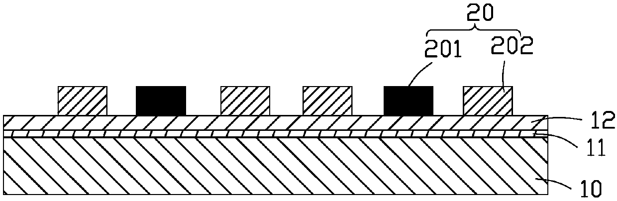
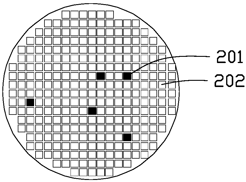
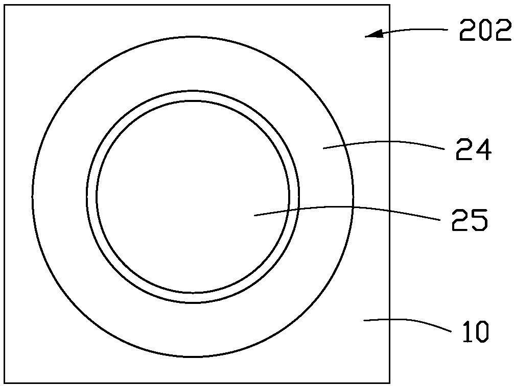
[0040] Step 1: See figure 1 A base substrate 10 is provided, a buffer layer 11 is formed on the base substrate 10 , and a laser blocking layer (UV blocking layer) 12 is formed on the surface of the buffer layer (Buffer Layer) 11 .

[0041] In this embodiment, the base substrate 10 is a sapphire substrate, and the buffer layer 11 and the laser blocking layer 12 are formed by metal organic chemical vapor deposition (MOCVD).

[0042] The material of the buffer layer 11 is aluminum nitride or gallium nitride, and the thickness of the buffer layer 11 is 10 nm to 50 nm, preferably, between 20 nm.

[0043] The material of the laser blocking layer 12 is doped gallium nitride or ...


PUM

PropertyMeasurementUnit
thicknessaaaaaaaaaa
thicknessaaaaaaaaaa
thicknessaaaaaaaaaa

Abstract

The invention relates to a manufacturing method of light-emitting diode micro-crystal grains. The method comprises the following steps of providing a substrate, wherein a buffer layer is formed on thesubstrate, and a laser blocking layer is formed on the surface of the buffer layer; forming array-arranged light-emitting diode micro-crystal grains on the laser blocking layer; providing an auxiliary substrate, and forming an adhesive layer on the auxiliary substrate; enabling the surface, having the adhesive layer, of the auxiliary substrate to be pressed to the light-emitting diode micro-crystal grains, wherein the gaps between the light-emitting diode micro-crystal grains are filled with the adhesive layer, and the adhesive layer is cured; performing irradiating on the substrate from thebottom surface of the substrate to enable the buffer layer to be gasified, wherein the substrate is separated from the laser blocking layer; performing etching on the substrate to remove the substrate; and performing dispergation on the adhesive layer so as to obtain a plurality of light-emitting diode micro-crystal grains.

Description

technical field [0001] The invention relates to an integrated circuit device manufacturing device, in particular to a method for manufacturing light-emitting diode microcrystal grains. Background technique [0002] Nowadays, in order to meet the needs of various high-density packaging, the semiconductor packaging industry has gradually developed various types of packaging designs. The semiconductor chips used for packaging come from wafers manufactured by fabs. The wafers have a semiconductor substrate And there are arrays of microcrystalline grains formed on its surface. [0003] In the prior art, before the good product die / chip is separated from the semiconductor substrate, it is necessary to ablate the bad die on the substrate (laser ablation). Due to the control and uniformity of the laser power, the die / chip The etching efficiency of the epitaxial layer is different, which may cause the problem that the ablation of the grain is not deep and remains or the ablation of ...

Claims


Application Information

Patent Timeline
Patent Type & Authority Applications(China)
IPC IPC(8): H01L33/48
CPCH01L33/0093H01L33/0095H01L33/38H01L33/007H01L33/32H01L2933/0016
Inventor 凃博闵洪梓健沈佳辉黄建翔彭建忠林雅雯邱镜学
Owner ZHANJING TECH SHENZHEN
Why Eureka
Try Eureka