Flexible display panel, preparation method of flexible display panel, and display device
A flexible display and manufacturing method technology, applied in identification devices, semiconductor/solid-state device manufacturing, instruments, etc., can solve problems such as difficult etching and removal of functional layers and the influence of flexible substrates
- Summary
- Abstract
- Description
- Claims
- Application Information
AI Technical Summary
Problems solved by technology
Method used
Image
Examples
Embodiment 1
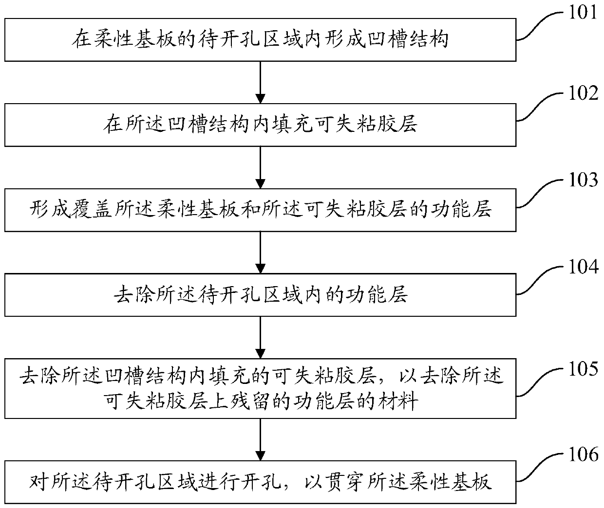
[0038] refer to figure 1 , which shows a flow chart of a method for manufacturing a flexible display panel according to an embodiment of the present invention, which may specifically include the following steps:
[0039] Step 101 , forming a groove structure in a region to be opened on the flexible substrate.
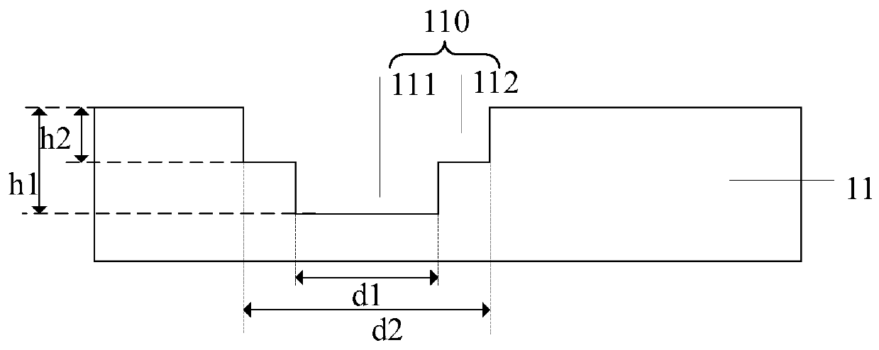
[0040] In the embodiment of the present invention, a groove structure is formed in the area to be opened reserved on the flexible substrate, and the groove structure may include only one groove, or may include multiple grooves.
[0041] When the groove structure only includes one groove, the plasma etching process is used to form a groove in the area to be opened on the flexible substrate, the depth of the groove is smaller than the thickness of the flexible substrate, for example, the groove can be The depth is set to 1 / 3-1 / 2 of the thickness of the flexible substrate, and the aperture of the groove is equal to the aperture of the area to be drilled.
[0042] When th...
Embodiment 2
[0066] An embodiment of the present invention provides a flexible display panel, which is manufactured by using the above method for manufacturing a flexible display panel.
[0067] Firstly, a groove structure 110 is formed in the area to be opened on the flexible substrate 11, and the removable adhesive layer 12 is filled in the groove structure 110. Then, the functional layer 13 is formed on the flexible substrate 11, so that the functional layer 13 covers the flexible substrate. The substrate 11 and the removable adhesive layer 12 are removed by etching the functional layer 13 in the area to be opened, and then the removable adhesive layer 12 filled in the groove structure 110 is removed, and the removed groove structure 110 is filled with When the removable adhesive layer 12 is used, the remaining functional layer material on the removable adhesive layer 12 can be removed at the same time, and finally, the area to be opened is etched to complete the opening to penetrate the...
PUM
| Property | Measurement | Unit |
|---|---|---|
| Thickness | aaaaa | aaaaa |
| Aperture | aaaaa | aaaaa |
| Peel strength | aaaaa | aaaaa |
Abstract
Description
Claims
Application Information


