Etching method and apparatus for a single wafer

An etching equipment and monolithic technology, which is applied in the direction of electrical components, semiconductor/solid-state device manufacturing, circuits, etc., can solve the problems of increased air flow, uneven etching of the edge, and damage to the chamfer shape of the edge

Inactive Publication Date: 2008-10-01
SUMCO CORP
View PDF1 Cites 12 Cited by
  • Summary
  • Abstract
  • Description
  • Claims
  • Application Information

AI Technical Summary

Problems solved by technology

[0010] However, when the gap between the rear surface of the wafer and the blowing mechanism on the lower surface is not suitable, the inventors have often found that the edge portion is not uniformly etched, and the chamfer shape of the edge portion is severely damaged, even if For example, the air flow from the blowing mechanism on the lower surface is adjusted to increase

Method used


Image

  • Etching method and apparatus for a single wafer
  • Etching method and apparatus for a single wafer
  • Etching method and apparatus for a single wafer

Examples


Embodiment 1

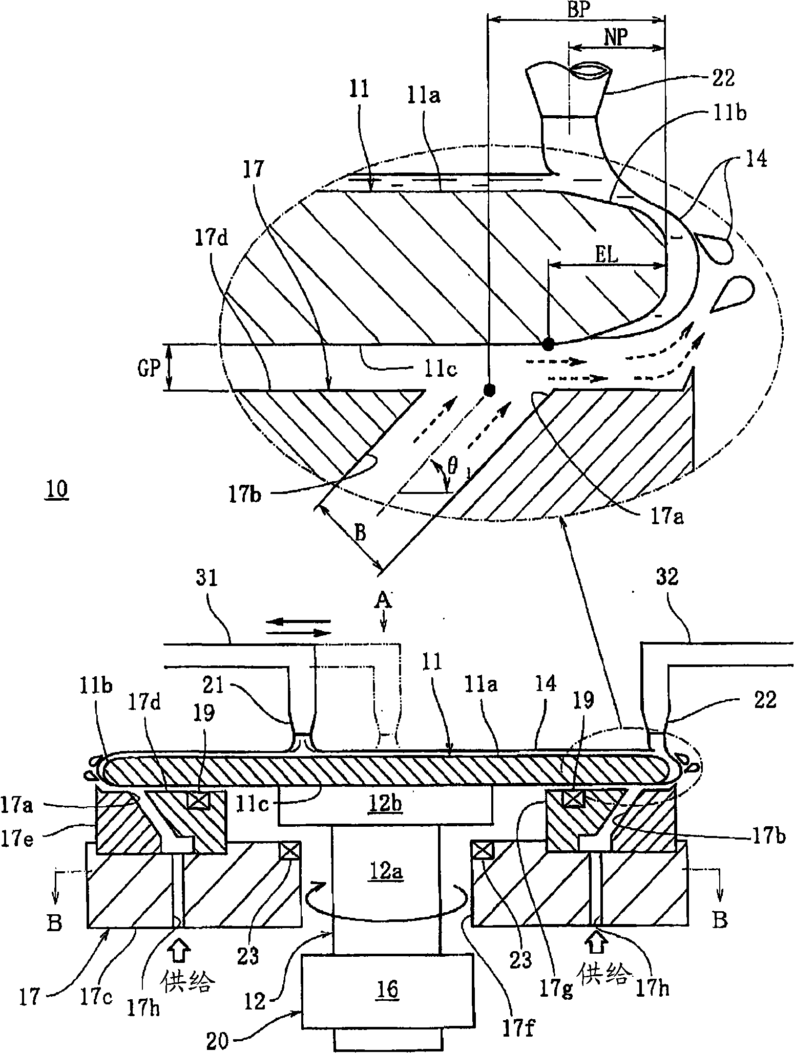
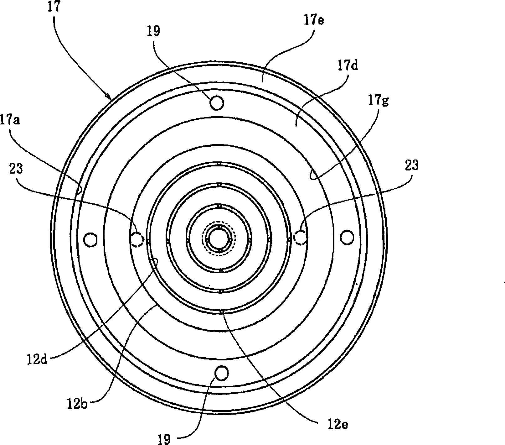
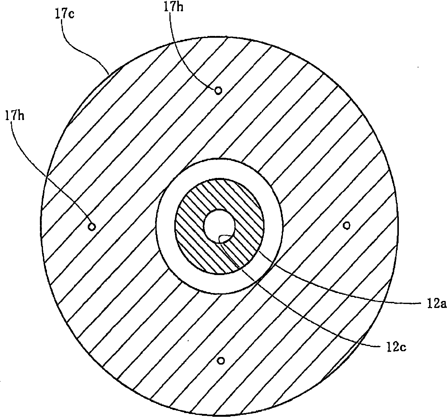
[0054] Such as figure 1 As shown, a monolithic etching apparatus 10 is used to etch a silicon wafer 11 having a diameter of 300 mm and a thickness of 0.8 mm. Here, the gap adjusting device 20 adjusts the gap GP between the upper surface of the lower surface blowing mechanism 17 and the lower surface 11c of the wafer 11 to 0.4mm, and the position BP of the ejection port 17a is set to be from the radially inner side of the wafer. The outer edge of the wafer is 3mm away from the position. In addition, the flow rate BF of the gas injected from the injection port 17a is set to 500 liters / minute, and G / B is set to 500, where G liters / minute is the flow rate of the gas from the injection port 17a, and Bmm is the injection port width. Moreover, the rotation speed of the wafer 11 was set to 400 rpm, and the angle θ formed by the spray groove 17b with respect to the horizontal plane was 1 Be set to 30 degrees, the flow rate of the etchant 14 ejected from the first nozzle 21 is set to...


PUM

PropertyMeasurementUnit
diameteraaaaaaaaaa
thicknessaaaaaaaaaa

Abstract

A single-wafer etching apparatus according to the present invention supplies an etchant to an upper surface of a wafer while rotating the wafer, thereby etching the upper surface of the wafer. Further, wafer elevating means moves up and down the wafer, and a lower surface blow mechanism which blows off the etchant flowing down on an edge surface of the wafer toward a radially outer side of the wafer by injection of a gas is fixed and provided without rotating together with the wafer. Furthermore, gap adjusting means controls the wafer elevating means based on detection outputs from gap detecting means for detecting a gap between the wafer and the lower surface blow mechanism, thereby adjusting the gap. The apparatus according to the present invention uniformly etches the edge portion without collapsing a chamfered shape of the edge portion of the wafer, and prevents a glitter from being produced on the edge surface of the wafer.

Description

technical field [0001] The present invention relates to a method of etching wafers one by one while rotating the wafers in a horizontal holding state and an etching device thereof. Background technique [0002] Generally, the semiconductor wafer manufacturing process includes the following steps: chamfering, mechanical polishing (grinding), etching, mirror polishing (grinding), and cleaning of wafers obtained by cutting and dividing single crystal ingots; thereby producing flat surfaces with high precision degree wafers. A wafer that has passed through a mechanical processing process such as block dicing, OD grinding, singulation or grinding has a damaged layer, ie a mechanically damaged layer on the upper surface of the wafer. A mechanically damaged layer causes crystal defects, ie, slip dislocations during device fabrication, reduces the mechanical strength of the crystal, and adversely affects the electrical properties, so this layer must be completely removed. An etchi...

Claims


Application Information

Patent Timeline
Patent Type & Authority Applications(China)
IPC IPC(8): H01L21/306H01L21/66C23F1/08
CPCH01L21/68735H01L21/67075H01L21/67063H01L21/67259H01L21/6708H01L21/306
Inventor 加藤健夫桥井友裕村山克彦古屋田荣高石和成
Owner SUMCO CORP
Why Eureka
Try Eureka