Fabrication method of Ti movable device

A manufacturing method and device technology, applied in the manufacture of microstructure devices, processes for producing decorative surface effects, coatings, etc., can solve problems such as poor fracture toughness, complex processes, large aspect ratio, etc., and achieve self-stress Small, uniform etching, bright surface effect

Inactive Publication Date: 2009-06-03
PEKING UNIV
View PDF0 Cites 12 Cited by
  • Summary
  • Abstract
  • Description
  • Claims
  • Application Information

AI Technical Summary

Problems solved by technology

There is also the use of SCREAM (single crystalreactive etching and metalisation) technology to realize the movable structure, but this method is more complicated and difficult to achieve a larger aspect ratio
At the same time, as a structural material, silicon has its own shortcomings such as poor conductivity and poor fracture toughness. If there is contact and friction on the surface of the device, its reliability is not good.
At

Method used


Image

  • Fabrication method of Ti movable device
  • Fabrication method of Ti movable device
  • Fabrication method of Ti movable device

Examples


Example Embodiment

[0037] Example 1: Using SU8 as the middle layer bonding

[0038] 1. Preparation of Titanium Substrate and Mask Generation

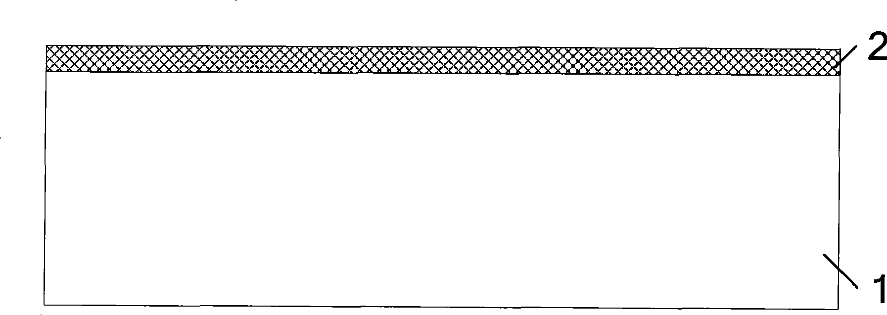
[0039] Such as figure 1 As shown, the device material is titanium. After annealing and chemical mechanical polishing, the surface of the titanium substrate is smooth and bright. The mask uses SU8 photoresist. SU8 is a kind of thick glue, and different thicknesses can be obtained at different speeds. Determine the mask thickness according to the required thickness of the device. In this embodiment, it is expected that the device height is 40 microns, and it is recommended to use SU8-3010 without dilution at a rotation speed of 1000 revolutions to obtain a thickness of about 15 microns.

[0040] 2. Define the mask pattern

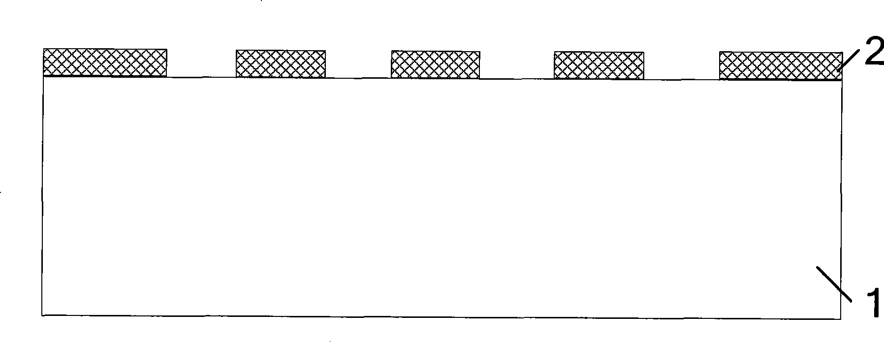
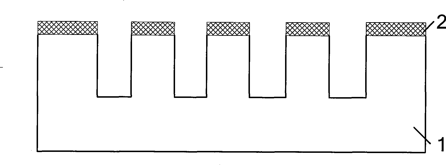
[0041] The pattern is defined by photolithography and development. After pre-baking, exposure, development, and post-exposure baking (Post ExposureBake), a mask pattern with flat and steep sidewalls can be obtained, such as figure 2 Shown....

Example Embodiment

[0053] Example 2 Using BCB as the middle layer bonding

[0054] Steps 1 to 6 are the same as in the first embodiment. In step 7, a benzocyclobutene polymer (BCB, Benzocyclobutene) is used as the intermediate layer, and the pattern is defined before the bonding. First coat BCB on the bonded glass, then use photoresist as a mask to define the BCB pattern, and use the plasma dry etching method to etch the BCB pattern, and then proceed to combine it with step 6 to obtain The titanium substrate is bonded with patterns, such as Picture 10 Shown. The subsequent steps are similar to the first embodiment. In the final structural release process, only the filled Parylene material needs to be removed with oxygen plasma.


PUM


Abstract

The invention discloses a fabrication method of a Ti movable device. The fabrication method comprises the following steps: etching a Ti substrate by plasma etching technology to form a deep groove, and filling the deep groove; bonding the Ti substrate with another substrate; thinning the back of the Ti substrate by chemical corrosion and chemical mechanical polishing until the deep groove is exposed; removing the filler in the deep groove; and releasing the movable structure to obtain a Ti micro-device with the movable structure. The method can achieve high-accuracy and high-aspect-ratio 3D processing of Ti on a plurality kinds of substrates, and can be used for processing a plurality of MEMS devices. The entire process adopts micro-electronic processing method, and has the advantages of high accuracy and uniform etching. The fabricated device has the advantages of bright surface, smooth sidewall, flat surface and small stress.

Description

technical field [0001] The invention belongs to the technical field of microelectromechanical system (MEMS) processing, and in particular relates to a microfabrication method of a metal titanium movable device based on deep etching technology. Background technique [0002] At present, the movable structure with high aspect ratio in the mainstream silicon-based MEMS technology is widely used in various sensors and drivers. The obtained devices have high working efficiency, large capacitor plate area, large driving force, small occupied chip area, and high power carrying capacity. The degree of integration is high. The traditional silicon-based processing method is realized by using KOH back cavity etching combined with ICP deep etching, so the back cavity occupies a large area. Another common method is to use SOI sheet directly for processing. There is also the use of SCREAM (single crystalreactive etching and metalisation) technology to realize the movable structure, but t...

Claims


Application Information

Patent Timeline
IPC IPC(8): B81C1/00
Inventor 陈兢赵刚
Owner PEKING UNIV
Why Eureka
Try Eureka