

Laminated wafer and manufacturing method thereof
A technology for bonding wafers and manufacturing methods, which is applied in semiconductor/solid-state device manufacturing, electrical components, electrical solid-state devices, etc., can solve problems such as thick oxide films, and achieve the effect of reducing the number of steps
- Summary
- Abstract
- Description
- Claims
- Application Information
AI Technical Summary
Problems solved by technology
Method used
Image

Examples
Embodiment 1
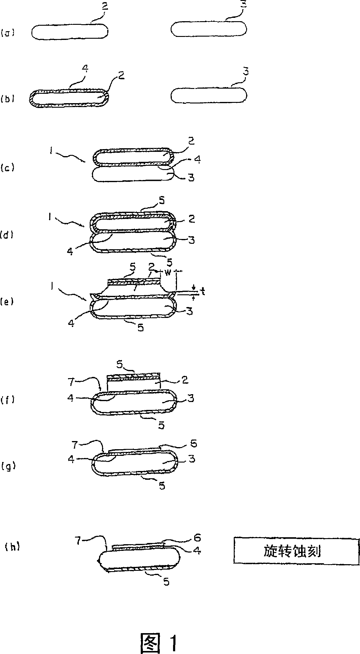
[0097] First, mirror-polished CZ wafers with a diameter of 200 mm, conductivity type p-type, and resistivity of 4-6 Ω·cm were prepared as base wafers and bonded wafers. Next, these wafers were closely attached according to the steps (a) to (c) in Figure 1, and bonded and heat-treated for 3 hours at 1150°C in an oxygen atmosphere to manufacture the bonded wafer as shown in Figure 1(d). Circle 1.
[0098] Next, as shown in FIG. 1( e ), the outer peripheral portion of the bonded wafer 2 is ground from the outer peripheral direction of the wafer toward the center using a grinding device. The thickness t is 50 micrometers.
[0099] Next, the unbonded portion of the outer peripheral portion of the bonded wafer 2 is removed by etching. The etchant for this etching uses NaOH, and the entire wafer is immersed in NaOH for etching. The etching amount was 90 microns, and the wafer shown in Fig. 1(f) was obtained.
[0100] Next, the surface of the bonding wafer 2 is ground and polished...
Embodiment 2
[0105] First, mirror-polished CZ wafers with a diameter of 200 mm, a conductivity type of p-type, and a resistivity of 4-6 Ω·cm were prepared as base wafers and bonding wafers, respectively. Next, a 5-micron oxide film was formed on the base wafer as shown in FIG. 5, and the Si layer bonded to the wafer was transferred to the base wafer using the SMART CUT method (registered trademark) to obtain an SOI wafer. Subsequently, a stabilizing heat treatment is performed.
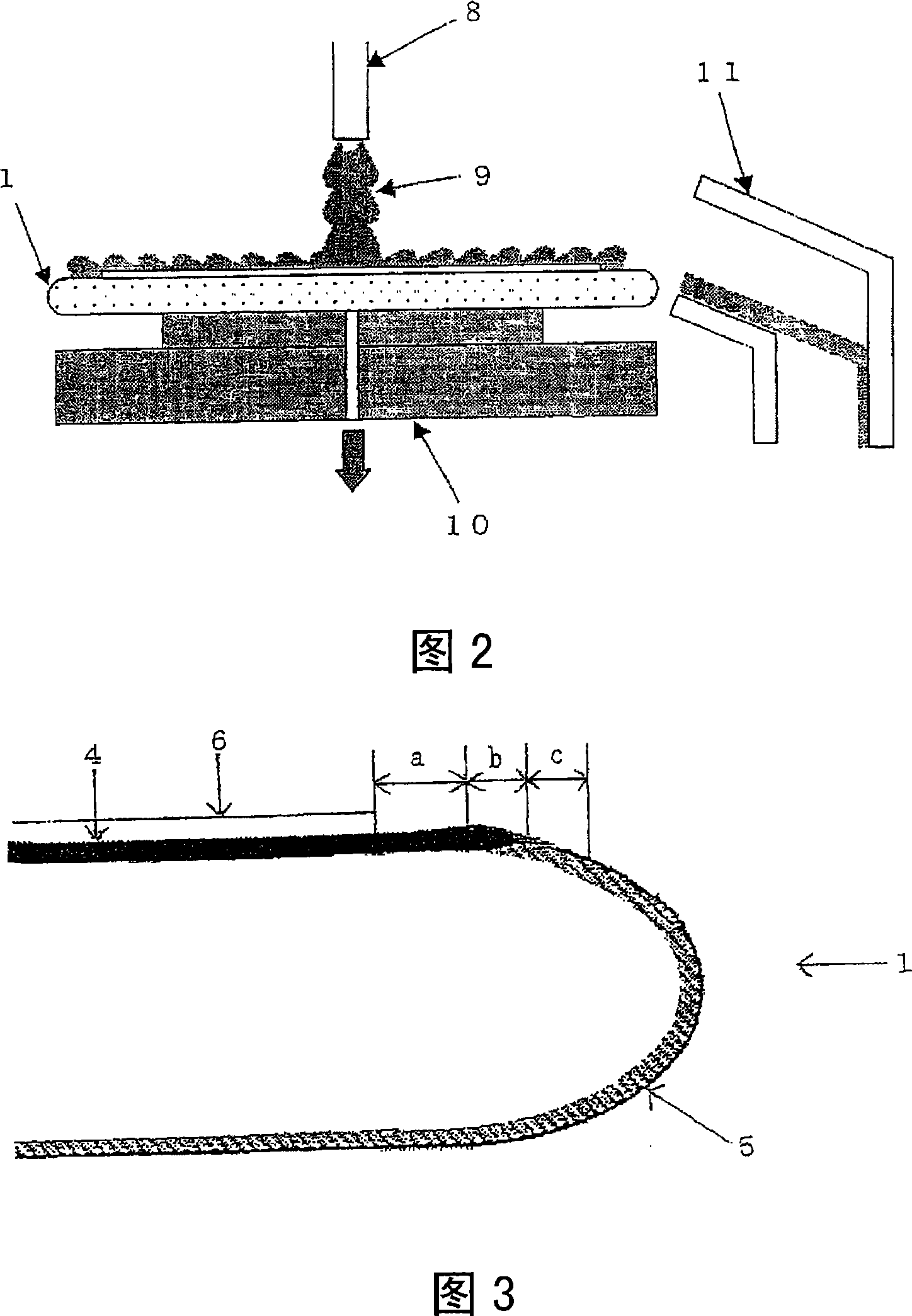
[0106] At this time, since an oxide film of 5 micrometers was present on the terrace portion of the SOI wafer, the oxide film was removed by spin etching using the apparatus shown in FIG. 6 . A 50% HF aqueous solution was used as an etching solution, and the etching solution was directly supplied to the terrace portion for 5 minutes to remove the oxide film on the terrace portion. In addition, during the spin etching, pure water is supplied as the protective fluid 12 to the central portion of the SOI wafer to pre...
Embodiment 3
[0110] First, mirror-polished CZ wafers with a diameter of 200 mm, a conductivity type of p-type, and a resistivity of 4-6 Ω·cm were prepared as base wafers and bonding wafers, respectively. Next, a 400nm oxide film was formed on the base wafer as shown in FIG. 5, and the Si layer bonded to the wafer was transferred to the base wafer using the SMART CUT method (registered trademark) to obtain an SOI wafer. Subsequently, a stabilizing heat treatment is performed.
[0111] At this time, since an oxide film of 400 nm was present on the terrace portion of the SOI wafer, the oxide film was removed by spin etching using the apparatus shown in FIG. 6 . A 50% HF aqueous solution was used as an etching solution, and the etching solution was directly supplied to the terrace portion for 1 minute to remove the oxide film on the terrace portion. In addition, during the spin etching, pure water is supplied as the protective fluid 12 to the central portion of the SOI wafer to prevent the et...
PUM
 Abstract
Description
Claims
Application Information