Organic electroluminescent device, display substrate and display device

An electroluminescent device and electroluminescent technology, which is applied in the direction of organic semiconductor devices, electro-solid devices, electrical components, etc., can solve the problems of high power consumption of OLED, high device driving voltage and low efficiency, etc.

Active Publication Date: 2019-05-17
BOE TECH GRP CO LTD +1
View PDF7 Cites 2 Cited by
  • Summary
  • Abstract
  • Description
  • Claims
  • Application Information

AI Technical Summary

Problems solved by technology

[0004] The present invention aims at the problems of low efficiency of existing OLED devices, high device driving voltage, and high OLED power consumption, and provides an organic electroluminescent device, a display substrate, and a display device

Method used


Image

  • Organic electroluminescent device, display substrate and display device
  • Organic electroluminescent device, display substrate and display device
  • Organic electroluminescent device, display substrate and display device

Examples


Embodiment 1

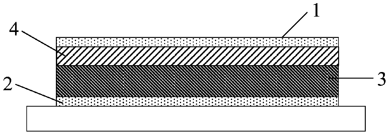
[0029] This embodiment provides an organic electroluminescent device, such as figure 1 As shown, it includes a first electrode 1, a second electrode 2, and a light-emitting layer 3 disposed between the first electrode 1 and the second electrode 2; a space is provided between the first electrode 1 and the light-emitting layer 3 The hole transport layer 4, the hole transport layer 4 includes a hole transport material and a P-type dopant material; wherein, the electrons of the highest occupied molecular orbital (HOMO) of the P-type dopant material can be excited by light, Excited to the lowest unoccupied molecular orbital (LUMO) of the P-type dopant material, so that an electron transfer reaction occurs from the highest occupied molecular orbital (HOMO) of the hole transport material to the highest occupied molecular orbital (HOMO) of the P-type dopant material , to realize the injection of hole carriers from the P-type dopant material to the hole transport material.

[0030] In...

Embodiment 2

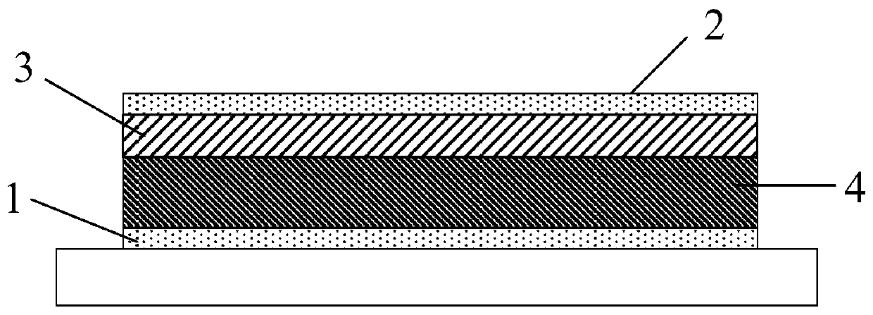
[0032] This embodiment provides an organic electroluminescent device, such as figure 2 As shown, it includes a first electrode 1, a second electrode 2, and a light-emitting layer 3 disposed between the first electrode 1 and the second electrode 2; a space is provided between the first electrode 1 and the light-emitting layer 3 The hole transport layer 4, the hole transport layer 4 includes a hole transport material and a P-type dopant material; wherein, the electrons of the highest occupied molecular orbital (HOMO) of the P-type dopant material have a wavelength of 380-780nm Under the excitation of a range of light, it is excited to the lowest unoccupied molecular orbital (LUMO) of the P-type dopant material, so that the highest occupied molecular orbital (HOMO) of the hole transport material to the highest occupied molecular orbital of the P-type dopant material (HOMO) undergoes an electron transfer reaction to realize the injection of hole carriers from the P-type dopant ma...

Embodiment 3

[0048] This embodiment provides a method for preparing the organic electroluminescent device of the above embodiment, comprising the following preparation steps:

[0049] S01. Form the first electrode; in this embodiment, the first electrode is used as an anode as an example for illustration, and the material for forming the anode may be one or a mixed alloy material of Al, Ag, Mg.

[0050] Optionally, a step of forming a pixel-defining structure may also be included, and the material of the pixel-defining structure may be selected from resin, polyimide, organic silicon or silicon dioxide. Wherein, the pixel definition structure defines a plurality of pixel units.

[0051] S02, using a hole transport material and a P-type dopant material to form a hole transport layer; wherein, the electrons of the highest occupied molecular orbital (HOMO) of the P-type dopant material can be excited to the P-type under the excitation of light The lowest unoccupied molecular orbital (LUMO) of...


PUM


Abstract

The invention provides an organic electroluminescent device, a display substrate and a display device and belongs to the field of display technology. The organic electroluminescent device can solve the problem that an existing OLED has relatively low efficiency, relatively high driving voltage and relatively high power consumption. In the organic electroluminescent device provided by the invention, a P type doping material of a hole transport layer does not need a deep LUMO energy level, hole carrier injection on the hole transport layer is realized by utilizing an electron transfer reaction performed on the P type doping material when the P type doping material is excited by lights, anode contact resistance is effectively reduced, hole injection is increased, voltage is reduced, efficiency of the organic electroluminescent device is improved, and power consumption is reduced.

Description

technical field [0001] The invention belongs to the field of display technology, and in particular relates to an organic electroluminescent device, a display substrate and a display device. Background technique [0002] At present, organic electroluminescent display devices (Organic Electroluminescent Display, OLED) have gradually become the mainstream in the display field due to their excellent performances such as low power consumption, high color saturation, wide viewing angle, thin thickness, and flexibility. [0003] The efficiency of the existing OLED device is low, the driving voltage of the device is relatively high, and the power consumption of the OLED is relatively high. Contents of the invention [0004] The invention aims at the problems of low efficiency of the existing OLED device, high device driving voltage and high power consumption of the OLED, and provides an organic electroluminescent device, a display substrate and a display device. [0005] The tech...

Claims


Application Information

Patent Timeline
Patent Type & Authority Applications(China)
IPC IPC(8): H01L51/50H01L27/32
CPCH10K85/611H10K85/311H10K85/322H10K50/155H10K50/11H10K59/35H10K71/13H10K71/30H10K71/135H10K71/164H10K85/30H10K2101/40H10K2101/30
Inventor 于天成
Owner BOE TECH GRP CO LTD
Why Eureka
Try Eureka