Fan-out type packaging structure and packaging method of chip

A technology of packaging structure and packaging method, which is applied in the direction of semiconductor/solid-state device parts, semiconductor devices, electrical components, etc., can solve the problems affecting the warpage of the package body, and achieve the effect of reducing package deformation warpage and controlling product warpage

Pending Publication Date: 2019-05-21
NAT CENT FOR ADVANCED PACKAGING
View PDF0 Cites 4 Cited by
  • Summary
  • Abstract
  • Description
  • Claims
  • Application Information

AI Technical Summary

Problems solved by technology

[0002] In the chip packaging process in the prior art, such as the fan-out packaging structure, it is a manually reconstructed wafer, and the reconstructed wafer contains plastic, silicon and metal materials, and the volume edge sum and thermal expansion coefficient between silicon and plastic The difference in each direction of X, Y, and Z will lead to the warpage of the package due to thermal expansion and contraction when the process is heated and cooled

Method used


Image

  • Fan-out type packaging structure and packaging method of chip
  • Fan-out type packaging structure and packaging method of chip
  • Fan-out type packaging structure and packaging method of chip

Examples


Embodiment Construction

[0021] The technical solutions of the present invention will be clearly and completely described below in conjunction with the accompanying drawings. Apparently, the described embodiments are some of the embodiments of the present invention, but not all of them. Based on the embodiments of the present invention, all other embodiments obtained by persons of ordinary skill in the art without making creative efforts belong to the protection scope of the present invention.

[0022] In addition, the technical features involved in the different embodiments of the present invention described below may be combined with each other as long as there is no conflict with each other.

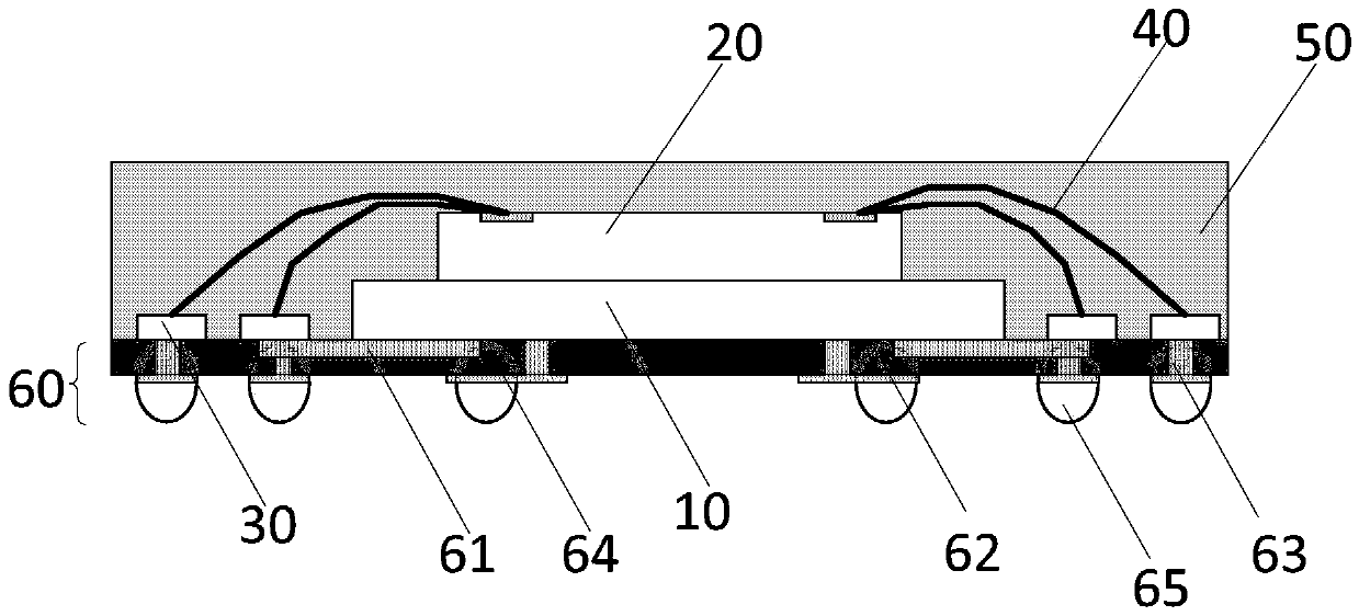
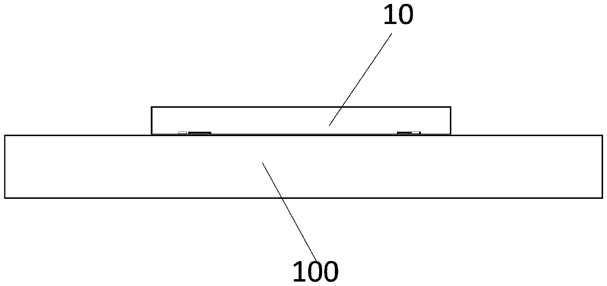
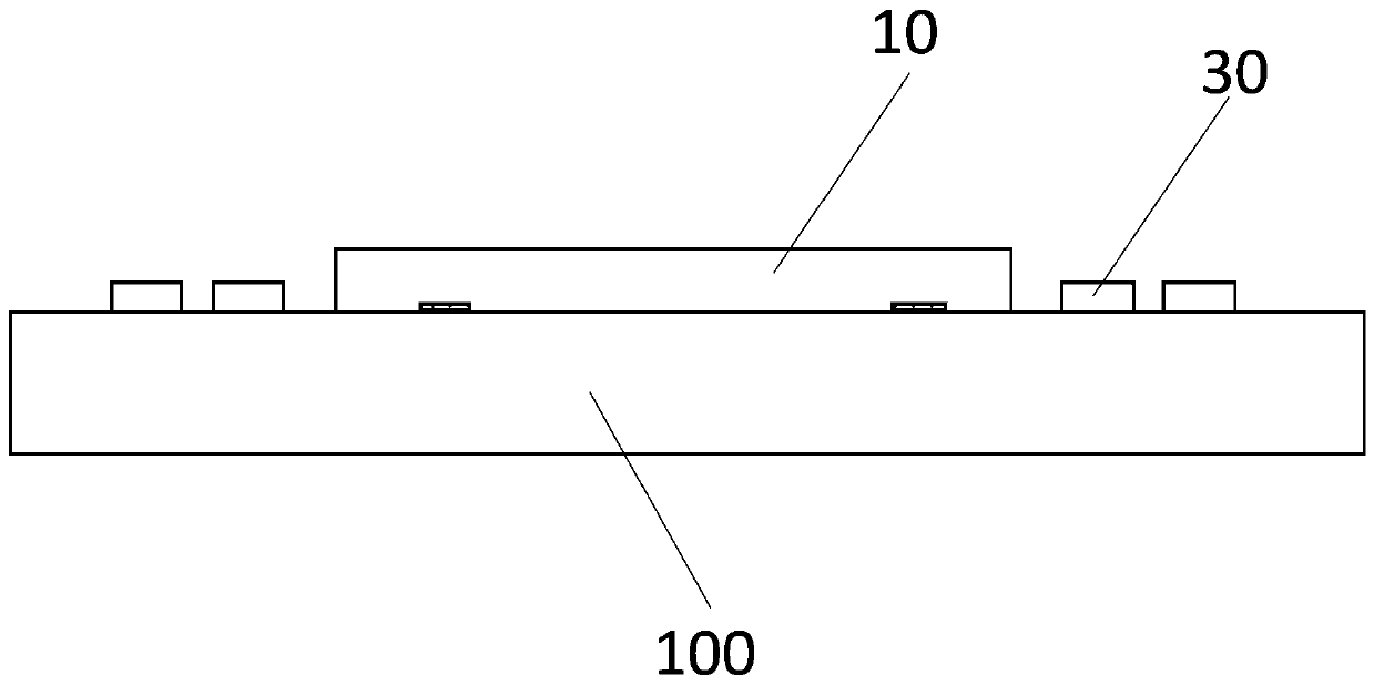
[0023] An embodiment of the present invention provides a chip fan-out packaging structure, such as figure 1 As shown, the structure includes: a first chip 10 and a second chip 20 whose bottom surfaces are relatively bonded; a plurality of metal terminals 30 are distributed around the first chip 10, and one si...


PUM


Abstract

The invention discloses a fan-out type packaging structure and packaging method of a chip; the fan-out type packaging structure comprises a first chip, a second chip, a plurality of metal terminals, alead, a packaging layer, and an extraction layer; the bottom surface of the first chip and the bottom surface of the second chip are oppositely attached to each other; the plurality of metal terminals are distributed on the periphery of the first chip, one face of the metal terminal is located on the same plane as the front surface of the first chip; the lead is connected between the front face of the second chip and the other face of the metal terminal; the packaging layer is used for packaging the first chip, the second chip, the lead and the metal terminals; and the extraction layer is arranged on a first surface of the packaging layer and is respectively electrically connected with one face of the metal terminal and / or the front face of the first chip. Compared with the fan-out type packaging structure packaged by using a slide glass whole surface, a plurality of metal terminals are arranged in a distributed mode, the packaging structure is balanced by utilizing the volume ratio of the metal terminals, for example, the numerical value of the equivalent thermal expansion coefficient of the packaging body is reduced, so that warping of the product is controlled, and packaging deformation warping is reduced. In addition, signal interconnection of multi-chip stacked in the Z direction can be realized through the plurality of metal terminals.

Description

technical field [0001] The invention relates to the technical field of semiconductor packaging, in particular to a chip fan-out packaging structure and packaging method. Background technique [0002] In the chip packaging process in the prior art, such as the fan-out packaging structure, it is a manually reconstructed wafer, and the reconstructed wafer contains plastic, silicon and metal materials, and the volume edge sum and thermal expansion coefficient between silicon and plastic The difference in each direction of X, Y, and Z will cause the warpage of the package due to thermal expansion and contraction when the process is heated and cooled. Contents of the invention [0003] Therefore, the present invention provides a chip fan-out packaging structure, which reduces the warpage of the packaging body. [0004] According to the first aspect, an embodiment of the present invention provides a chip fan-out packaging structure, at least including: a first chip and a second ...

Claims


Application Information

Patent Timeline
Patent Type & Authority Applications(China)
IPC IPC(8): H01L23/482H01L23/498H01L21/48
CPCH01L2924/15311H01L2924/181H01L2224/18H01L2224/48227H01L2224/32145H01L2224/73267H01L2224/73265H01L23/49541H01L23/49575H01L21/568H01L23/49816H01L23/5384H01L21/4857H01L2224/96H01L2224/85001H01L2224/48247H01L2224/04105H01L2224/12105H01L25/0657H01L25/50H01L2225/0651H01L2225/06568H01L24/19H01L2924/00012H01L2924/00H01L21/4853H01L21/565H01L21/6835H01L23/3128H01L23/5383H01L23/5386H01L24/20H01L2221/6835H01L2224/214H01L2225/06524H01L2225/06586
Inventor 孙鹏任玉龙
Owner NAT CENT FOR ADVANCED PACKAGING
Why Eureka
Try Eureka