A single pulse generation circuit and a bidirectional level conversion circuit
A technology for generating circuits and single pulses, which is applied in the direction of logic circuits, pulse technology, logic circuit connection/interface layout, etc., can solve the problems of destroying the impedance matching of output ports and large power consumption, so as to speed up signal transmission speed and reduce power consumption. Loss, ensure the effect of impedance matching and signal integrity
- Summary
- Abstract
- Description
- Claims
- Application Information
AI Technical Summary
Problems solved by technology
Method used
Image

Examples
Embodiment Construction
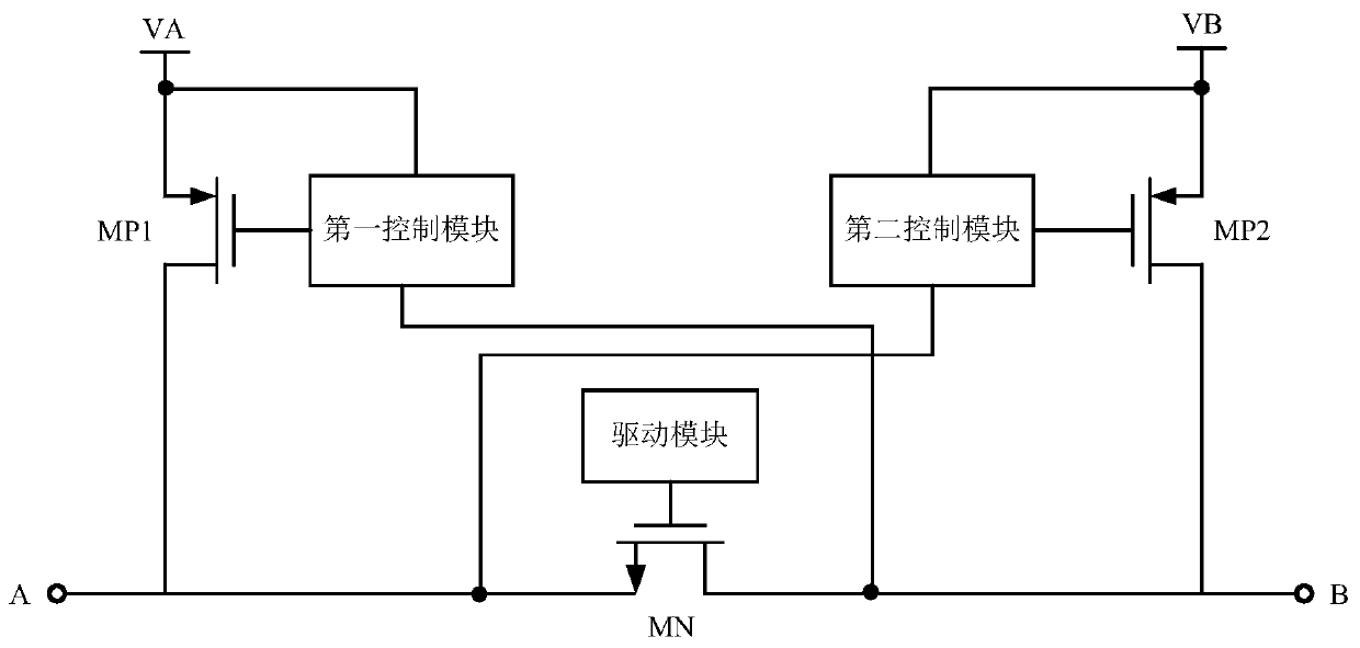
[0044] As mentioned in the background, in the existing level shifting chip, the pull-up control module will cause a large power consumption of the chip. Such as figure 1 as shown, figure 1 It is a structural schematic diagram of an existing level conversion chip. When the first terminal A of the signal transmission terminal MN is turned from a low level to a high level, the second control module controls the second pull-up transistor MP2 to turn on, and the signal The second terminal B of the transmission terminal MN is pulled from a low level to a high level; when the second terminal B of the signal transmission terminal MN is turned from a low level to a high level, the first control module controls the first pull-up transistor MP1 to conduct is turned on, the first terminal A of the signal transmission terminal MN is pulled from low level to high level.
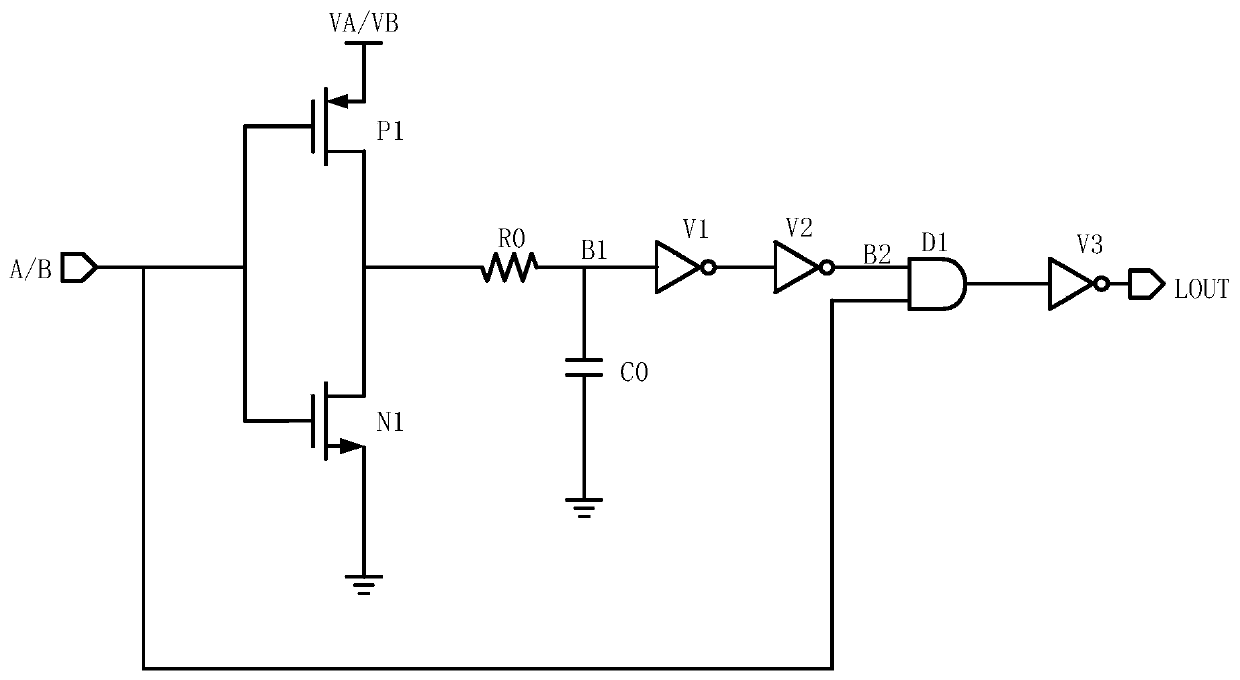
[0045] Such as figure 2 as shown, figure 2 It is a structural schematic diagram of an existing control module. Whe...
PUM
 Abstract
Description
Claims
Application Information
 - R&D
- Intellectual Property
- Life Sciences
- Materials
- Tech Scout
- Unparalleled Data Quality
- Higher Quality Content
- 60% Fewer Hallucinations
Browse by: Latest US Patents, China's latest patents, Technical Efficacy Thesaurus, Application Domain, Technology Topic, Popular Technical Reports.
© 2025 PatSnap. All rights reserved.Legal|Privacy policy|Modern Slavery Act Transparency Statement|Sitemap|About US| Contact US: help@patsnap.com