Multi-turn arranged carrier-free IC (Integrated Circuit) chip packaging component and manufacturing method thereof

A technology of chip package and production method, which is applied in the fields of electrical solid-state devices, semiconductor devices, semiconductor/solid-state device manufacturing, etc., to achieve good high-frequency performance, good electrical performance, and the effect of improving test yield and reliability

Active Publication Date: 2011-11-02
TIANSHUI HUATIAN TECH +1
View PDF3 Cites 7 Cited by
  • Summary
  • Abstract
  • Description
  • Claims
  • Application Information

AI Technical Summary

Problems solved by technology

The current four-sided flat no-lead package cannot meet the needs of high-density, multi-I / O packaging due to fewer pins, that is, fewer I / Os. At the same time, the bonding wire is long, which affects high-frequency applications.
Moreover, the general thickness of QFN is controlled at 0.82mm~1.0㎜, which cannot meet the needs of ultra-thin packaging products.

Method used


Image

  • Multi-turn arranged carrier-free IC (Integrated Circuit) chip packaging component and manufacturing method thereof
  • Multi-turn arranged carrier-free IC (Integrated Circuit) chip packaging component and manufacturing method thereof
  • Multi-turn arranged carrier-free IC (Integrated Circuit) chip packaging component and manufacturing method thereof

Examples


Embodiment 1

[0055](1), wafer thinning thickness 250μm

[0056] Coarse grinding thickness range, from original wafer to final thickness + adhesive film thickness + 50 μm, rough grinding speed 5 μm / s; fine grinding thickness range, from final thickness + adhesive film thickness + 50 μm to final wafer thickness + adhesive film thickness , Grinding speed: 0.4μm / s, wafer thinning method ordinary QFN thinning, 6-inch to 8-inch wafer VG-502MKⅡ8B automatic thinning machine, 8-inch to 12-inch wafer adopts PG300RM / TCN;

[0057] (2), scribing

[0058] Wafers up to 8 inches use DISC3350 or double-knife dicing machines, and wafers from 8 inches to 12 inches use A-WD-300TXB dicing machines. Application of anti-fragmentation and anti-crack scribing software control technology, the scribing speed is controlled at ≤10mm / s;

[0059] (3), single chip flip chip and reflow soldering

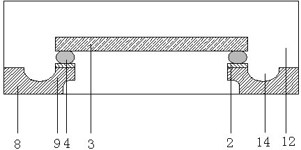
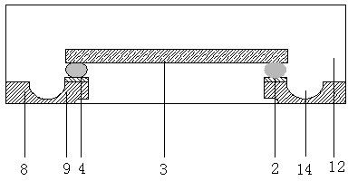
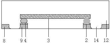
[0060] Single-chip flip-chip bonding, using IC chip 3 with bumps, flip-chip bonding is performed on a carrier frame with a ...

Embodiment 2

[0076] (1), wafer thinning thickness 250μm

[0077] Coarse grinding thickness range, from original wafer to final thickness + adhesive film thickness + 50μm, rough grinding speed 2μm / s; fine grinding thickness range, from final thickness + adhesive film thickness + 50μm to final wafer thickness + adhesive film thickness , Grinding speed: 0.9μm / s, ordinary QFN thinning method for wafer thinning, VG-502MKⅡ8B automatic thinning machine for 6-inch to 8-inch wafers, PG300RM / TCN for 8-inch to 12-inch wafers;

[0078] (2) Scribing

[0079] With embodiment 1;

[0080] (3), single chip flip chip and reflow soldering

[0081] With embodiment 1;

[0082] (4), bottom filling

[0083] Choose a material with a low thermal expansion coefficient, heat the underfill to 80°C, use vacuum technology to underfill the bumps 4 and the pins in the frame, and finally bake the finished product after the underfill in a QFN general-purpose baking oven Bake for about 15 minutes;

[0084] (5)~(7)

...

Embodiment 3

[0093] (1)~(7)

[0094] With embodiment 1;

[0095] (8), separate pins

[0096] The pins are separated from each other by laser cutting method, and the cutting depth is 0.13μm;

[0097] (9), electroplating

[0098] The electroplating is the same as that of ordinary QFN packages, directly plating 7μm pure tin in the electroless plating system, and the baking conditions and methods after electroless plating are the same as those of ordinary QFN packages after electroplating;

[0099] (10), cutting and separating products

[0100] With embodiment 1.


PUM


Abstract

The invention discloses a multi-turn arranged carrier-free IC (Integrated Circuit) chip packaging component and a manufacturing method thereof. The multi-turn arranged carrier-free IC chip packaging component comprises a lead frame, inner pins, an IC chip and a plastic packaging body, wherein the lead frame is a carrier-free lead frame, the inner pins of the lead frame are arranged around four sides of the lead frame in turns, the IC chip is provided with bumps, and the bumps are connected to the inner pins. The number of pins of the packaging component in the invention is increased by over 40% compared with the number of the pins of a single-row lead frame with the same area; and bonding lines are not needed for the connection of the pins and the lead frame, and the structure is simple and reasonable. The heat conduction distance is short, the heat performance is excellent, the inner welding inductance and capacitance of a circuit are reduced due to direct contact between the bumps and the frame (a base plate and a chip), the signal transmission is fast, the little distortion is caused, and the electric performance is excellent; in addition, the thickness and the weight of packaging are reduced, thus the crossing and the open circuit of bonding wires are avoided, and the test yield and reliability are improved.

Description

technical field [0001] The invention relates to the technical field of electronic information automation component manufacturing, in particular to four-sided flat leadless IC chip packaging, specifically a multi-circle arrangement carrierless IC chip package, and the invention also includes a production method of the package. Background technique [0002] In recent years, with the rapid development of portable electronic components in the field of mobile communications and mobile computers, small packaging and high-density assembly technology has been greatly developed; at the same time, a series of strict requirements have been put forward for small packaging technology, such as requirements The package dimensions should be kept as small as possible, especially if the package height is less than 1 mm. The reliability of the connection after packaging is improved as much as possible, which is suitable for lead-free soldering and effectively reduces costs. [0003] The inte...

Claims


Application Information

Patent Timeline
Patent Type & Authority Applications(China)
IPC IPC(8): H01L23/495H01L23/31H01L21/98
CPCH01L2224/16245
Inventor 朱文辉慕蔚李习周郭小伟
Owner TIANSHUI HUATIAN TECH
Why Eureka
Try Eureka