Manufacturing method of silicon germanium heterojunction bipolar transistor device

A technology of heterojunction bipolar and manufacturing method, which is applied in semiconductor/solid-state device manufacturing, electrical components, circuits, etc., and can solve problems such as low etching rate, affecting process stability, and large total width

Active Publication Date: 2022-06-21
SHANGHAI HUAHONG GRACE SEMICON MFG CORP
View PDF8 Cites 0 Cited by
  • Summary
  • Abstract
  • Description
  • Claims
  • Application Information

AI Technical Summary

Problems solved by technology

[0007] The above method can form a self-aligned HBT of non-selective germanium-silicon epitaxy; however, in the actual research and development process, the following problems were found. If the wall formation is etched to the silicon surface by a dry method, the subsequent growth of the selective outer base region will be uneven, and if the wet method is used by a dry method, the lower etching rate at the bottom will form a larger outer wall. The third is to sacrifice When the emitter is etched back, it is easy to form a fence-shaped residue on the edge of the polysilicon, which affects the stability of the process

Method used


Image

  • Manufacturing method of silicon germanium heterojunction bipolar transistor device
  • Manufacturing method of silicon germanium heterojunction bipolar transistor device
  • Manufacturing method of silicon germanium heterojunction bipolar transistor device

Examples


Embodiment Construction

[0045] Specific embodiments of the present invention are disclosed below; however, it is to be understood that the disclosed embodiments are merely exemplary of the invention, which may be embodied in various forms. Therefore, specific structural and functional details disclosed herein are not to be interpreted as limiting. Further, the terms and terms used herein are not limiting; rather, they provide an understandable description of the invention. The present invention will be better understood by considering the following description in conjunction with the accompanying drawings, wherein like reference numerals represent the same meaning. The drawings are not to scale.

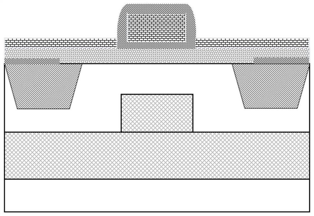
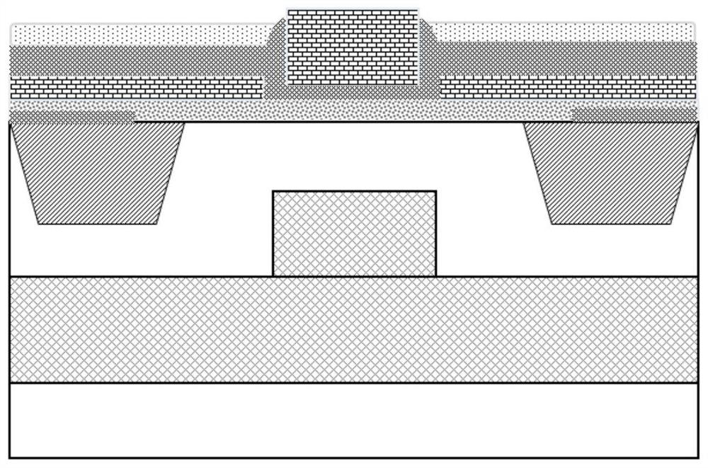
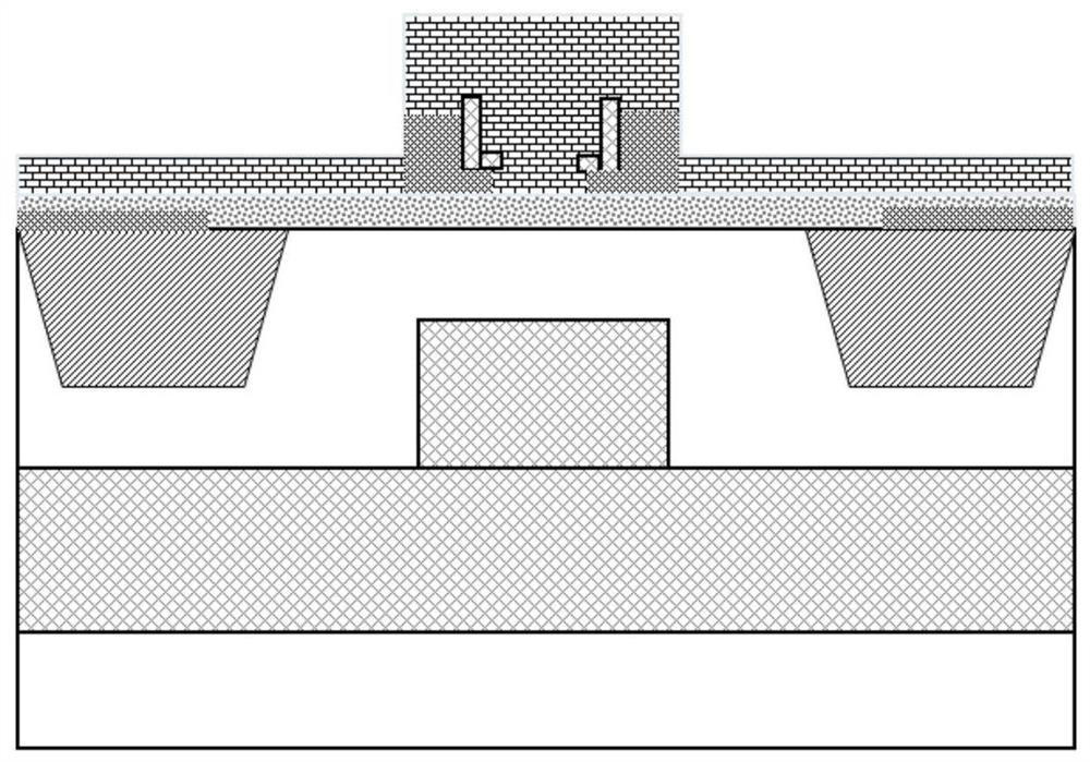
[0046] A manufacturing method of a silicon germanium heterojunction bipolar transistor device according to a preferred embodiment of the present invention includes the following steps:

[0047] step one, as Figure 4-5 As shown, after the collector electrode is formed and the non-selective SiGe base regi...


PUM

PropertyMeasurementUnit
thicknessaaaaaaaaaa
thicknessaaaaaaaaaa
thicknessaaaaaaaaaa

Abstract

The invention discloses a manufacturing method of a germanium-silicon heterojunction bipolar triode device, which adopts non-selective low-temperature germanium-silicon epitaxial growth, undergoes deposition and etching of sacrificial emitter polysilicon, and dry etching of the outer wall , Wet etching and cleaning, using the selective epitaxial method to form an elevated outer base region and outer wall, and then etch back the sacrificial emitter polysilicon, after cleaning, deposit the emitter polysilicon and dry etch, and finally form the emitter A self-aligned device in which polysilicon and polysilicon in the base area are separated by side walls; compared with the prior art, due to the use of primary side walls, smaller side walls can be formed, which can effectively reduce the series resistance of the base to improve The highest oscillation frequency of the device.

Description

technical field [0001] The invention relates to the field of semiconductor integrated circuits, in particular to a manufacturing method of a silicon germanium heterojunction bipolar transistor device. Background technique [0002] P-type polysilicon is used to raise the outer base region, and a self-aligned device structure with inner wall is used between the emitter and the outer base region, which can reduce the base resistance and the base-collector capacitance at the same time. Polar triode (HBT) devices can obtain the highest oscillation frequency fmax greater than 300GHz, and their performance can be comparable to III-V devices, and are widely used in optical communication and millimeter wave applications. [0003] In the prior art, sacrificial emitter window polysilicon is used, and processes such as planarization of organic media and engraving of inner and outer walls are performed. The specific steps are: [0004] After forming the collector, deposit a silicon oxid...

Claims


Application Information

Patent Timeline
Patent Type & Authority Patents(China)
IPC IPC(8): H01L21/331
Inventor 周正良
Owner SHANGHAI HUAHONG GRACE SEMICON MFG CORP
Why Eureka
Try Eureka