A pixel structure, display device, display device and projection display system

A technology of display device and pixel structure, which is applied in instruments, nonlinear optics, optics, etc., can solve problems such as low integration and complex structure, and achieve the effects of improving integration, simplifying structure, and reducing thickness

Active Publication Date: 2021-03-30
SHANXI UNIV
View PDF5 Cites 0 Cited by
  • Summary
  • Abstract
  • Description
  • Claims
  • Application Information

AI Technical Summary

Problems solved by technology

[0003] Existing display devices, such as figure 1 as shown, figure 1 It is a schematic diagram of the display principle of an existing liquid crystal display device. When no electric field is added between the upper and lower glass substrates, the incident light passes through the lower polarizer, that is, the polarizing layer 1, and follows the liquid crystal to make a 90-degree twist and passes through the upper polarizing plate, that is, the polarizing layer. 2 exit, so that the display device is displayed as a bright state; when an electric field is added between the upper and lower glass substrates, the liquid crystal molecules will rearrange so that the incident light is no longer twisted but maintains the original direction, and the outgoing light will be captured by the upper polarizer, that is, polarized light Layer 2 shielding cannot be seen through, making the display device appear in a dark state
That is to say, the existing display device needs to use the upper and lower polarizers to realize the modulation of the display brightness, which leads to the existing display device having a complicated structure and a low integration level.

Method used


Image

  • A pixel structure, display device, display device and projection display system
  • A pixel structure, display device, display device and projection display system
  • A pixel structure, display device, display device and projection display system

Examples


Embodiment Construction

[0058] The above is the core idea of ​​the present invention. In order to make the above-mentioned purposes, features and advantages of the present invention more obvious and easy to understand, the technical solutions in the embodiments of the present invention will be clearly and completely described below in conjunction with the accompanying drawings in the embodiments of the present invention Description, obviously, the described embodiments are only a part of the embodiments of the present invention, rather than all the embodiments. Based on the embodiments of the present invention, all other embodiments obtained by persons of ordinary skill in the art without making creative efforts belong to the protection scope of the present invention.

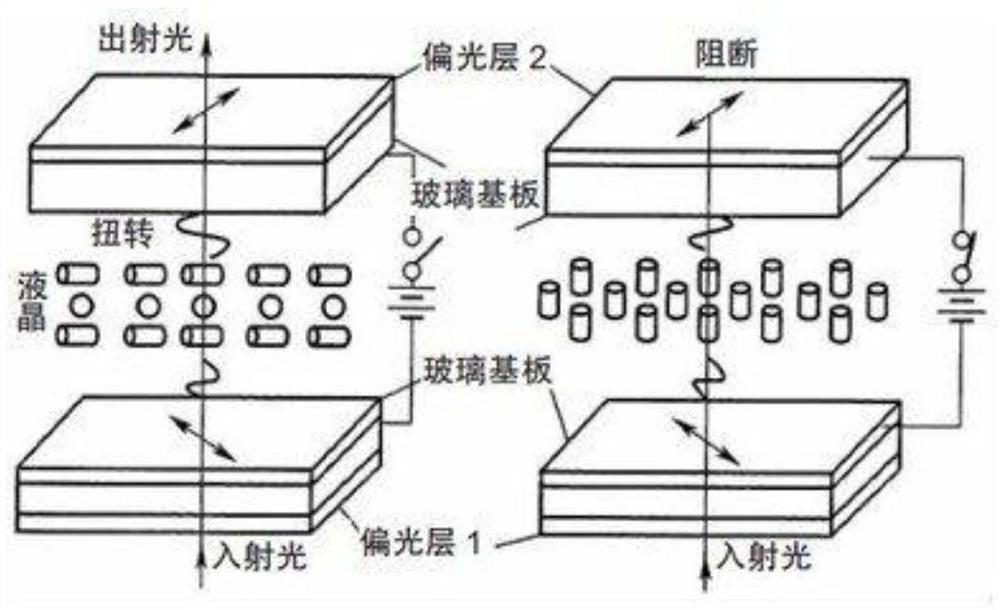
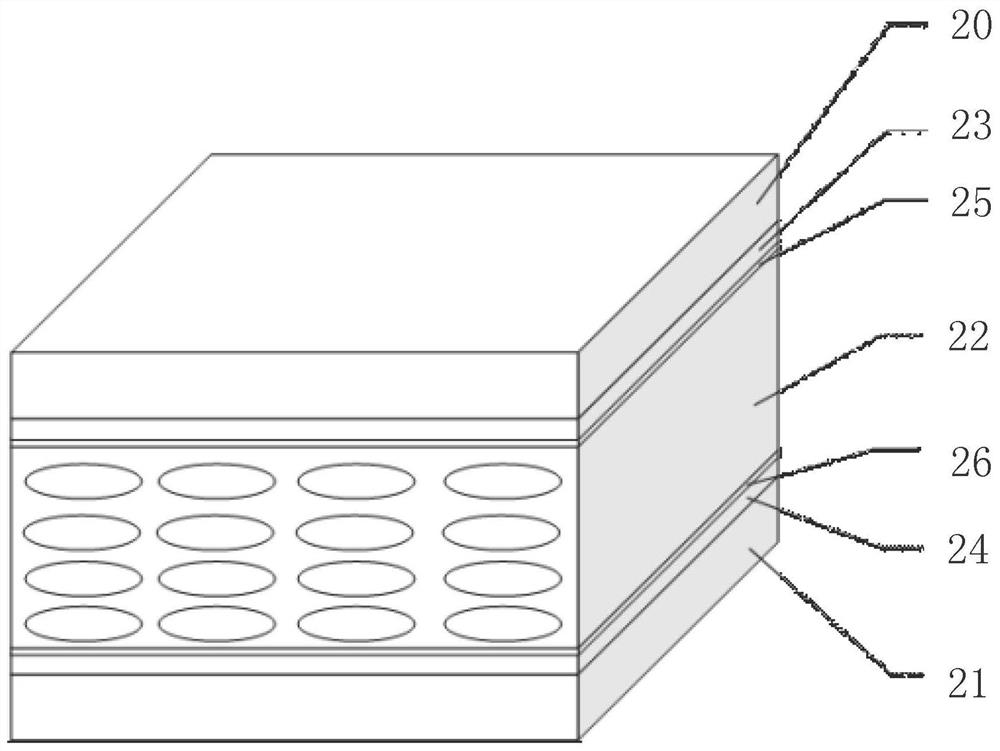
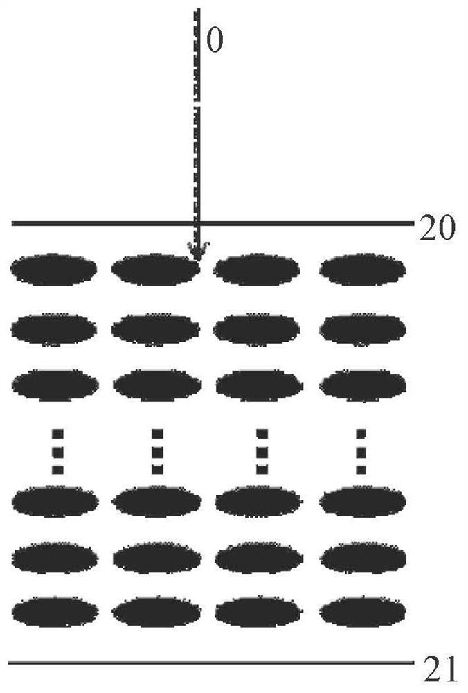
[0059] An embodiment of the present invention provides a pixel structure, such as figure 2 As shown, the pixel structure includes a first substrate 20, a second substrate 21, and a light-transmitting layer 22 between the first substr...


PUM

PropertyMeasurementUnit
emission peakaaaaaaaaaa
thicknessaaaaaaaaaa
thicknessaaaaaaaaaa

Abstract

To provide a pixel structure, a display device, a display and a projection display system which include a light-transmitting layer between a first substrate and a second substrate.SOLUTION: A first substrate 20 has a first reflection film 23 on a side facing toward a second substrate 21. The second substrate 21 has a second reflection film 24 on a side facing toward the first substrate 20. The first substrate 20 and the second substrate 21 form a Fabry-Perot cavity. The display luminance of a pixel structure is adjusted by adjusting the intensity of interference light of transmitted light or reflected light of the Fabry-Perot cavity.SELECTED DRAWING: Figure 2

Description

technical field [0001] The present invention relates to the field of display technology, and more specifically, to a pixel structure, a display device, a display device and a projection display system. Background technique [0002] 80% of the information that humans obtain from the external world comes from vision. Therefore, display devices are an important way for modern people to obtain information, and display technology is an important development direction in the information field. As people have more and higher requirements for information acquisition, they have more expectations for the performance of displays, and the research on display technology and devices is becoming more and more important. [0003] Existing display devices, such as figure 1 as shown, figure 1 It is a schematic diagram of the display principle of an existing liquid crystal display device. When there is no electric field added between the upper and lower glass substrates, the incident light p...

Claims


Application Information

Patent Timeline
Patent Type & Authority Patents(China)
IPC IPC(8): G02F1/1335G02F1/1337G02F1/1343G02F1/13357
Inventor 仝召民高权陈旭远
Owner SHANXI UNIV
Why Eureka
Try Eureka