GaN microrod array/graphene field emission cathode composite material preparation method

A technology of emitting cathode and composite material, which is applied in cold cathode manufacturing, electrode system manufacturing, discharge tube/lamp manufacturing, etc., can solve the problem of current uniformity and stability to be improved, difficulty in large current emission, and small electron affinity. and other problems, to achieve the effect of good field emission stability, low cost and simple preparation process

Inactive Publication Date: 2019-05-31
XIAN UNIV OF TECH
View PDF5 Cites 0 Cited by
  • Summary
  • Abstract
  • Description
  • Claims
  • Application Information

AI Technical Summary

Problems solved by technology

GaN microrods have the advantages of high melting point, high thermal conductivity, high breakdown voltage, and small electron affinity, and are increasingly used in field

Method used


Image

  • GaN microrod array/graphene field emission cathode composite material preparation method
  • GaN microrod array/graphene field emission cathode composite material preparation method
  • GaN microrod array/graphene field emission cathode composite material preparation method

Examples


preparation example Construction

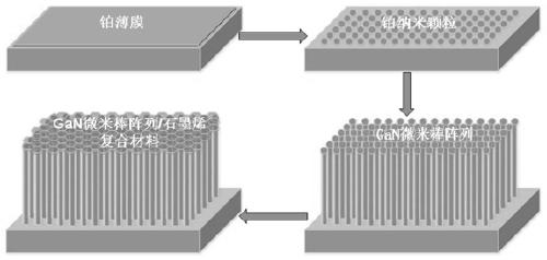
[0025] The invention provides a GaN microrod array / graphene field emission cathode composite material preparation method, the specific steps are as follows:

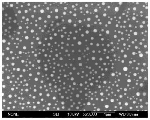
[0026] Step 1, using the JFC-1600 ion sputtering coater, the vacuum degree is 8×10 -3 In the case of Pa, set the sputtering current to 40-60mA, and the sputtering time to 40-80s, coat the silicon substrate with a platinum film, put the silicon substrate sputtered with a platinum film into a quartz boat, with the coating surface facing up, Then push the quartz boat into the constant temperature zone of the tube furnace and anneal the silicon substrate. Nitrogen was used to remove the air in the furnace tube for 20 minutes, and then the temperature was raised to 800-1200°C at a rate of 10°C per minute for annealing treatment, and naturally cooled to room temperature after annealing. Obtain substrate A;

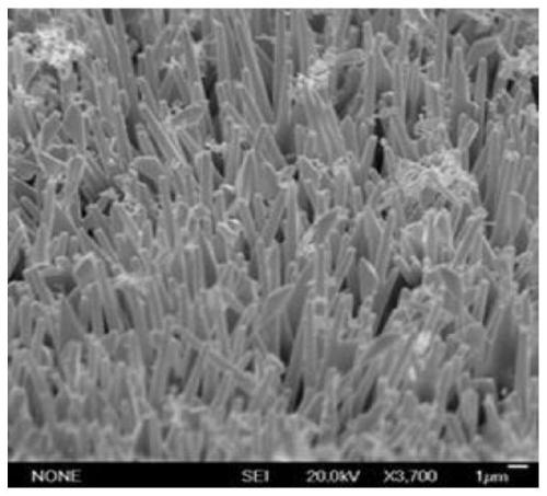
[0027] Step 2, move the substrate A obtained in step 1 into the quartz boat, use ammonia gas and gallium oxide as the ...

Embodiment 1

[0033] A GaN microrod array / graphene field emission cathode composite material preparation method, the specific steps are as follows:

[0034] Step 1, using the JFC-1600 ion sputtering coater, the vacuum degree is 8×10 -3 In the case of Pa, set the sputtering current to 40mA and the sputtering time to 40s, and coat the silicon substrate with a platinum film. Push it into the constant temperature zone of the tube furnace to anneal the silicon substrate. Set the annealing temperature to 800°C, the flow rate of ammonia gas to 50 sccm, and the annealing time to 5 minutes. , and then heat up to 800°C at a rate of 10°C per minute for annealing, and naturally cool to room temperature after annealing to obtain a substrate A;

[0035] Step 2, move the substrate A obtained in step 1 into the quartz boat, use ammonia gas and gallium oxide as the nitrogen source and gallium source, first place the carbon powder and gallium oxide in the quartz boat at a ratio of 1:1, and then place the su...

Embodiment 2

[0038] A GaN microrod array / graphene field emission cathode composite material preparation method, the specific steps are as follows:

[0039] Step 1, using the JFC-1600 ion sputtering coater, the vacuum degree is 8×10 -3 In the case of Pa, set the sputtering current to 60mA and the sputtering time to 80s, coat the silicon substrate with a platinum thin film, put the silicon substrate sputtered with a platinum thin film into a quartz boat with the coated surface facing up, and then put the quartz boat Push it into the constant temperature zone of the tube furnace to anneal the silicon substrate. Set the annealing temperature to 1200°C, the flow rate of ammonia gas to 200 sccm, and the annealing time to 30 minutes. , and then heat up to 1200°C at a rate of 10°C per minute for annealing, and naturally cool to room temperature after annealing. Obtain substrate A;

[0040] Step 2, move the substrate A obtained in step 1 into the quartz boat, use ammonia gas and gallium oxide as ...


PUM

PropertyMeasurementUnit
Diameteraaaaaaaaaa
Diameteraaaaaaaaaa

Abstract

The invention discloses a GaN microrod array/graphene field emission cathode composite material preparation method. The method comprises the following steps of step1, plating a platinum thin film on asilicon substrate, carrying out annealing processing on the silicon substrate plated with the platinum thin film, and after annealing, naturally cooling to a room temperature to obtain a substrate A;step2, carrying out heat processing on the substrate A obtained in the step 1 and a reaction source, keeping a certain distance between the substrate A and the reaction source, and after a reaction is completed, naturally cooling to the room temperature to obtain a substrate B; and step3, carrying out heat processing on the substrate B obtained in the step 2, and after the reaction is completed,naturally cooling to the room temperature so as to obtain a GaN microrod array/graphene field emission cathode composite material. The GaN microrod array/graphene field emission cathode composite material prepared by the method has an excellent field emission characteristic.

Description

technical field [0001] The invention belongs to the technical field of composite material preparation methods, and in particular relates to a preparation method of a GaN microrod array / graphene field emission cathode composite material. Background technique [0002] Field emission, also known as cold cathode emission or self-electron emission, is a phenomenon in which electrons are emitted from the surface of an object under the action of a strong electric field. Narrowing, or using an internal strong electric field to make electrons enter the dielectric layer from the base layer, and accelerate in the dielectric layer to obtain greater energy, so that the electrons inside the object do not need to obtain additional energy, that is, they can escape without exciting the electrons. phenomenon. With the continuous development of vacuum microelectronics in the field of display applications, field emission display (FED) technology has become an important research topic. The key...

Claims


Application Information

Patent Timeline
IPC IPC(8): H01J9/02C23C14/16C23C14/34C23C14/58C23C16/26C23C16/30C23C16/44
Inventor 崔真王霞赵娜娜李恩玲王少强
Owner XIAN UNIV OF TECH
Why Eureka
Try Eureka