
Preparation method of large surface area carbon nano pipe film for field emitting display cathode

A carbon nanotube film, carbon nanotube technology, applied in semiconductor devices, electroluminescent light sources, electrical components, etc., can solve the problems of limited and uniform substrate materials, equipment investment and product manufacturing costs, and achieve good alignment. , Large area uniformity, low cost effect

Inactive Publication Date: 2007-01-03
XI AN JIAOTONG UNIV
View PDF2 Cites 0 Cited by
  • Summary
  • Abstract
  • Description
  • Claims
  • Application Information

AI Technical Summary

Problems solved by technology

But it also has the following problems: due to the high growth temperature, suitable substrate materials are limited, and it is difficult to maintain uniformity on a large area; when growing a large-area cathode film, the investment in equipment and product manufacturing costs will increase significantly

Method used

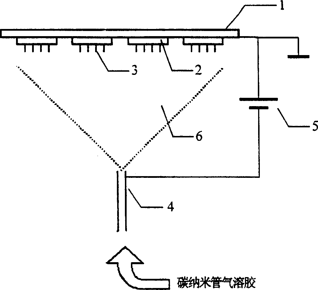
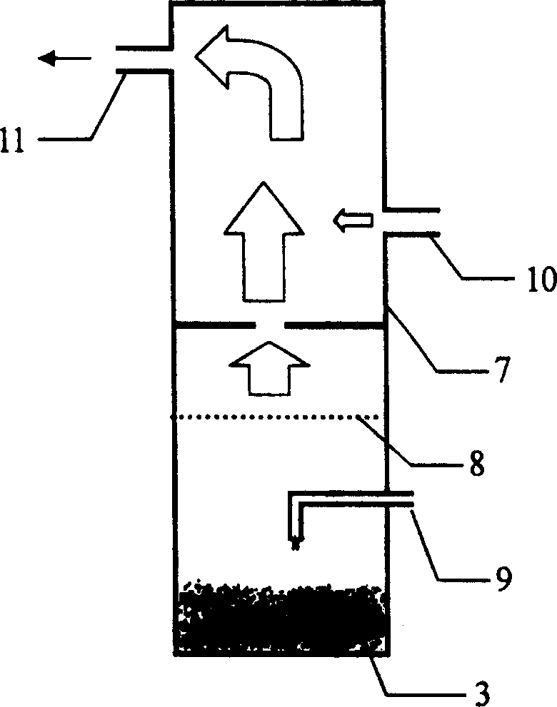

Image

  • Preparation method of large surface area carbon nano pipe film for field emitting display cathode
  • Preparation method of large surface area carbon nano pipe film for field emitting display cathode
  • Preparation method of large surface area carbon nano pipe film for field emitting display cathode

Examples


preparation example Construction

[0032] Since the catalyst used in the preparation process of carbon nanotubes will exist in carbon nanotubes, it should be removed during use. The specific process is to use concentrated nitric acid to dissolve the catalyst present in the carbon nanotubes in the preparation process of the carbon nanotubes; wash with distilled water to neutrality and then fully dry, and then use a ball mill to fully grind in a dry environment to reduce larger agglomerated particles;

[0033] (3) Formation of cathode conductive pattern

[0034] The required cathode pattern can be obtained by performing photolithography and etching on the conductive layer by common photolithography process. For substrate materials without a conductive layer on the surface, the required pattern can be obtained by plate making and printing.

[0035] (3) Coating adhesive

[0036] The adhesive can be coated on the cathode conductive pattern by screen printing or electrostatic spraying. The layout of the screen pla...

Embodiment 1

[0051] Embodiment 1: manufacture has the parallel strip cathode of the small field emission flat panel display of X-Y addressing

[0052] Its manufacturing process is as follows:

[0053] 1. Substrate selection and pretreatment

[0054] In this embodiment, glass with an ITO conductive layer (hereinafter referred to as ITO glass) is used as the substrate. Put the selected glass into a cleaning solution mixed with absolute alcohol and acetone at a volume ratio of 1:1, perform ultrasonic cleaning for 15 minutes, then ultrasonically clean it with deionized water for 15 minutes, and dry it in a clean environment. Dry and set aside.

[0055] 2. Pretreatment of carbon nanotubes

[0056] The carbon nanotubes used in this embodiment are multi-walled carbon nanotubes prepared by CVD, which contain a lot of impurities mainly including catalyst particles (mainly iron and its oxides). Its pretreatment is mainly to remove these impurities therein, and then make carbon nanotube powder wi...

Embodiment 2

[0067] Embodiment 2: manufacture the parallel strip cathode of the elongated field emission flat panel display with X-Y addressing

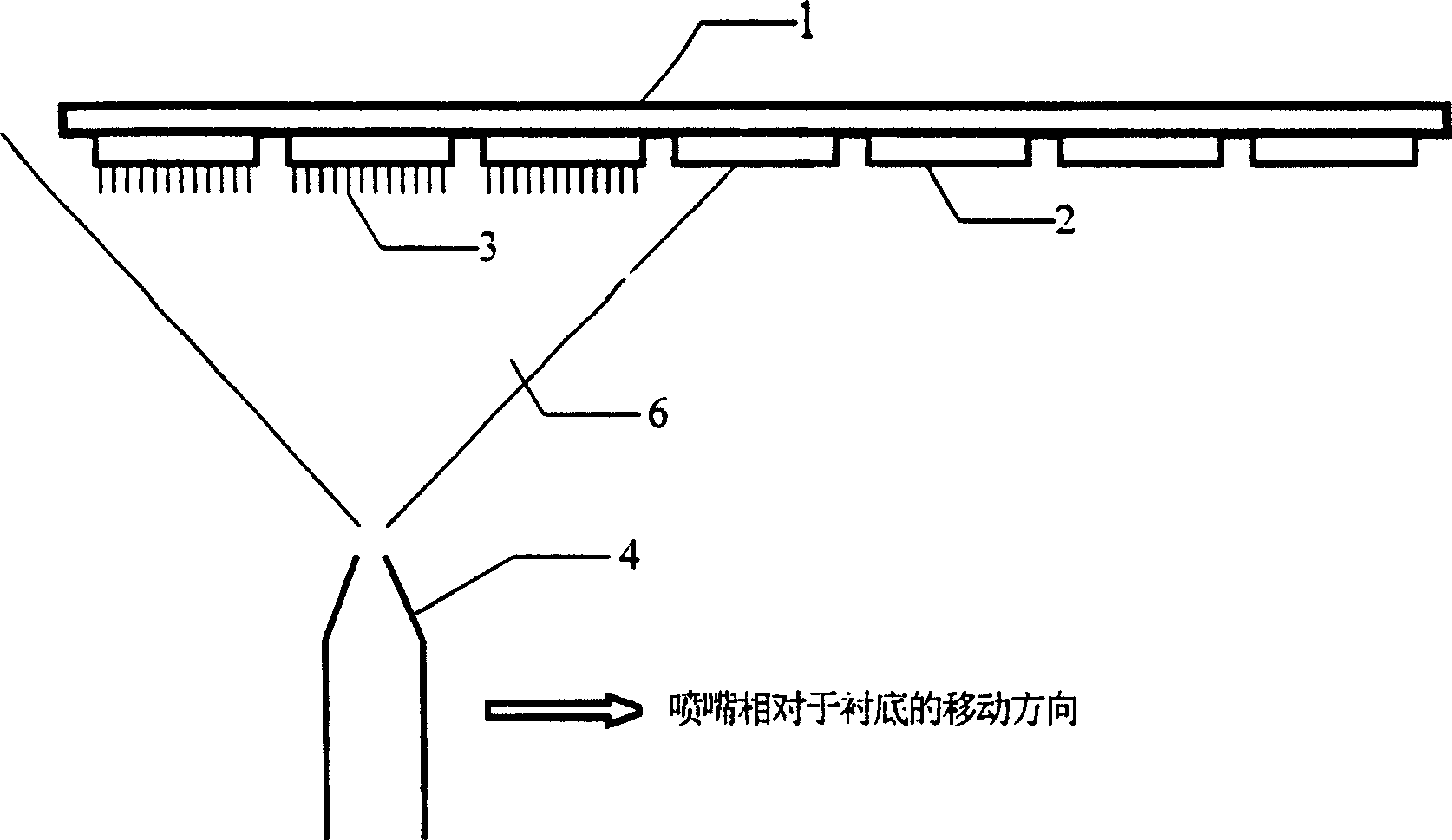
[0068] The manufacturing process of this embodiment is the same as that of Embodiment 1, except that a moving nozzle system is used in step 5. Of course, the preparation can also be completed by spraying with nozzle arrays.


PUM


Abstract

The invention discloses a method for manufacturing large-area carbon nanometer tube film negative electrode applied to field monitor. The method includes: preprocessing of substrate and the carbon nanometer tube, formation of negative electrode conductive figure, painting bonding agent, formation and spraying of carbon nanometer tube gas sol (or other type of disperse phase), depositing of the carbon nanometer on the substrate, drying and baking of the carbon nanometer tube film. The depositing density of the carbon nanometer tube film can be changed through adjusting content and depositing time of the carbon nanometer tube in the disperse phase; depositing shape of the film can be changed through adjusting the distribution of static electric field; the negative electrode of large-scale screen carbon nanometer tube field transmitting flat monitor can be produced by using a moving nozzle system or multiple nozzle system. The method provided by the invention is simple, the cost is low, and the product can be produced in the open area. The acquired carbon nanometer tube film has an even area, excellent arrangement, simple domain.

Description

technical field [0001] The invention belongs to the intersection field of vacuum microelectronics technology and nanotechnology, and specifically relates to using the electrostatic field and the self-charge distribution of charged carbon nanotubes to implant carbon nanotubes on the surface of a substrate in an orientation, forming at least one jump barrier or surface The invention relates to a method for preparing a field emission cathode of a potential barrier, in particular to a method for preparing a large-area carbon nanotube thin film used for a cathode of a field emission display. Background technique [0002] At present, the cathode preparation technology of carbon nanotube field emission display mainly includes screen printing technology and direct growth technology. The screen printing method has the advantage of simple operation, but is limited in the manufacture of high-resolution display panels. In this method, carbon nanotubes are usually mixed with slurry-maki...

Claims


Application Information

Patent Timeline
Patent Type & Authority Patents(China)
IPC IPC(8): H01L33/00H05B33/00
Inventor 朱长纯曾凡光刘卫华李玉魁
Owner XI AN JIAOTONG UNIV
Learn More