
Method for improving warping of intelligent power semiconductor module product by using mould

A smart power and semiconductor technology, applied in semiconductor devices, semiconductor/solid-state device manufacturing, electric solid-state devices, etc., to achieve the effects of improving product warping, avoiding glue overflow, and avoiding adverse effects

Inactive Publication Date: 2019-06-07
TIANSHUI HUATIAN MICROELECTRONICS
View PDF5 Cites 3 Cited by
  • Summary
  • Abstract
  • Description
  • Claims
  • Application Information

AI Technical Summary

Problems solved by technology

[0004] The invention discloses a method for improving warpage of an intelligent power semiconductor module product by using a mold. Using the mold of the invention, the warpage of an intelligent power semiconductor module product can be improved, which solves the problem that cannot be effectively solved in the prior art, and avoids product warpage. many adverse effects, especially to effectively avoid the problem of glue overflow

Method used


Image

  • Method for improving warping of intelligent power semiconductor module product by using mould
  • Method for improving warping of intelligent power semiconductor module product by using mould
  • Method for improving warping of intelligent power semiconductor module product by using mould

Examples


Embodiment 1

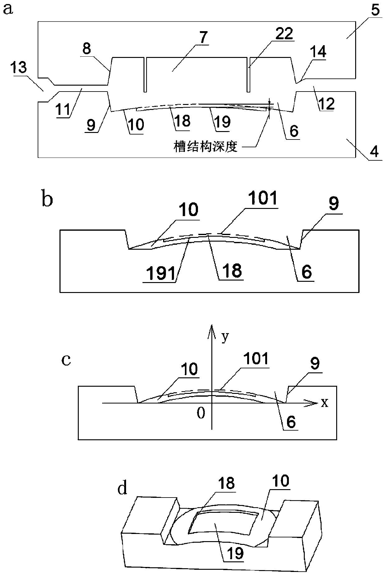
[0041] see attached image 3, where a is a schematic diagram of the structure of the method of using a mold to improve the warpage of an intelligent power semiconductor module product, b is a schematic diagram of the groove structure under the method of using a mold to improve the warpage of an intelligent power semiconductor module product, and c is the use of a mold to improve the warpage of the intelligent power semiconductor module product. Schematic diagram of the groove with coordinate axis structure under the bending method, d is the schematic diagram of the three-dimensional structure of the groove under the method of using molds to improve the warpage of smart power semiconductor module products (for the sake of simplicity and clarity, the funnel-shaped representation is omitted from the left end of b, c, and d. , and the long side of the groove under the lower mold for injection molding is omitted, which does not affect the understanding of those skilled in the art. A...

Embodiment 2

[0046] On the basis of the first embodiment, the bottom surface of the upper groove is designed as an upward spherical surface 15, and the equation of the arc at the junction of the spherical surface 15 and the vertical plane (perpendicular to the horizontal plane) is y=-2.29×10 -4 x 2 +0.22, the midpoint of the line connecting the center points of the two short sides of the bottom surface of the above groove is the coordinate origin, the height of the spherical surface is 0.22 mm, the length is 62 mm consistent with the length of the bottom surface of the upper groove, and the width is the same as the bottom surface of the upper groove. The width is the same as 32 mm; the rest is the same as the first embodiment, see the appendix Figure 8 . According to the existing intelligent power semiconductor modules, the thickness of the lower mold where the heat dissipation substrate is located is smaller than that of the upper mold. First, it is easier to dissipate heat. Second, the...

Embodiment 3

[0049] On the basis of the first embodiment, the bottom surface of the upper groove is designed as a downward spherical surface 16; the equation of the arc at the junction of the spherical surface 16 and the vertical plane (perpendicular to the horizontal plane) is y=1.95×10 -4 x 2 -0.2, the midpoint of the line connecting the center points of the two short sides of the bottom surface of the above groove is the coordinate origin, the height of the spherical surface is 0.2 mm, the length is 64 mm consistent with the bottom surface length of the upper groove, and the width is the same as the bottom surface of the upper groove. The width is uniformly 34 mm; the upper surface of the spherical surface 16 is also provided with a groove structure 20, and the rest are the same as in the first embodiment, see appendix Figure 10 .

[0050] The intelligent power semiconductor module product with double-sided heat dissipation structure obtained by the above mold is shown in the appendix...


PUM

PropertyMeasurementUnit
Depthaaaaaaaaaa

Abstract

The invention provides a method for improving the warping of an intelligent power semiconductor module product by using a mould. In short, the intelligent power semiconductor module is arranged in themould, and packaged through injection molding, so that the improvement of the warping of the intelligent power semiconductor module product is finished. The mould comprises an injection lower mould and an injection upper mould; the injection lower mould is provided with a lower groove; the injection upper mould is provided with an upper groove; the bottom surface of the lower groove is provided with a spherical surface facing upwards; the lower groove and the upper groove define an injection molding cavity; the bottom surface of the upper groove is provided with a spherical surface facing upwards, or the bottom surface of the upper groove is provided with a spherical surface facing downwards, or the bottom surface of the upper groove is a plane; the surface of the spherical structure at the bottom surface of the lower groove is provided with a groove structure; the bottom surface of the groove structure is spherical; and the injection upper mould is provided with an ejector pin. According to the method, the purpose of improving the warping of the intelligent power semiconductor module product can be achieved with no need of changing or adding any packaging process, and especiallythe excessive glue phenomenon is avoided.

Description

technical field [0001] The invention relates to equipment for preparing intelligent power semiconductor module products, in particular to a method for improving the warpage of intelligent power semiconductor module products by using molds. Background technique [0002] Smart power semiconductor module products are often exposed to high temperature environments during the manufacturing process. However, due to the difference in thermal expansion coefficient (CTE mismatch) between the heat dissipation substrate and the encapsulation resin, the heat dissipation substrate and the encapsulation resin often have different degrees of thermal expansion and cause stress. pull, resulting in warping. [0003] The warpage problem of smart power semiconductor module products often causes many adverse effects, such as the situation that the product may break the chip material or even the chip due to deformation; When the product is subjected to external stress, the heat dissipation subst...

Claims


Application Information

Patent Timeline
IPC IPC(8): B29C45/26B29C45/14H01L21/56
CPCH01L2224/48137H01L2224/73265H01L2924/181H01L2224/32225H01L2924/3511H01L2924/00012
Inventor 孙炎权崔卫兵蒋卫娟
Owner TIANSHUI HUATIAN MICROELECTRONICS
Learn More