Display panel and preparation method thereof

A technology for display panels and substrates, which is applied in the manufacture of semiconductor/solid-state devices, semiconductor devices, electrical components, etc., can solve the problems of complex process and high cost, and achieve the effect of simplifying the manufacturing process, reducing the manufacturing cost, and preventing spillover.

Inactive Publication Date: 2019-06-07
KUNSHAN GO VISIONOX OPTO ELECTRONICS CO LTD
View PDF6 Cites 2 Cited by
  • Summary
  • Abstract
  • Description
  • Claims
  • Application Information

AI Technical Summary

Problems solved by technology

[0004] However, the height, width and position of the embankment obtained by the above method of manufacturing the embankment are fixed. If the shape

Method used


Image

  • Display panel and preparation method thereof
  • Display panel and preparation method thereof
  • Display panel and preparation method thereof

Examples


Embodiment Construction

[0045] The present invention will be further described in detail below in conjunction with the accompanying drawings and embodiments. It should be understood that the specific embodiments described here are only used to explain the present invention, but not to limit the present invention. In addition, it should be noted that, for the convenience of description, only some structures related to the present invention are shown in the drawings but not all structures.

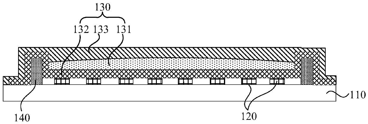
[0046] figure 1 It is a schematic structural view of a display panel provided by an embodiment of the present invention, and the display panel includes: a base substrate 110; a plurality of organic light emitting devices 120 disposed on the upper surface of the base substrate 110; a thin film encapsulation layer 130, and a thin film encapsulation layer 130 It is arranged on the side of the base substrate 110 close to the organic light emitting device 120, and encapsulates a plurality of organic light emitting devi...


PUM


Abstract

The present invention discloses a display panel and a preparation method thereof. The display panel comprises: a substrate; a plurality of organic light-emitting modules arranged at the upper surfaceof the substrate; a film package layer arranged at one side, close to the organic light-emitting modules, of the substrate and packaged with organic light-emitting devices, wherein each organic light-emitting module comprises at least one organic layer and at least one inorganic layer which are stacked; and a dam comprising at least one frame-shaped structure, wherein the dam is arranged around the organic layer and attached to one side, close to the organic light-emitting devices, of the substrate so as to flexibly regulate the dam size, the attachment position and the dam quantity accordingto the size of the display panel when the dam is attached to so as to simplify the preparation process of the display panel, reduce the manufacturing device and effectively block the overflow of the organic layer materials in the film package layer after attachment of the dam.

Description

technical field [0001] Embodiments of the present invention relate to the field of display technology, and in particular to a display panel and a manufacturing method thereof. Background technique [0002] An organic light emitting diode (Organic Light Emitting Diode, OLED) display device has the advantages of self-illumination, wide viewing angle, etc., so it is more and more widely used in the display field. [0003] Since the electrodes and organic layers of the organic light emitting display device are easily corroded by water, oxygen, etc., the service life of the display device is reduced, and the organic light emitting display device needs to be packaged. When encapsulating an organic light-emitting display device, it is necessary to arrange dams at the edge of the display panel to prolong the intrusion path of water, oxygen, and the like. In the prior art, the dams are usually completed during the fabrication of the organic light-emitting element array, and are obta...

Claims


Application Information

Patent Timeline
IPC IPC(8): H01L51/52H01L51/56
Inventor 金凤杰敖伟王明晖
Owner KUNSHAN GO VISIONOX OPTO ELECTRONICS CO LTD
Why Eureka
Try Eureka