

Package structure of optical sensors and package method of optical sensors
An optical sensor and packaging structure technology, applied in the field of sensors, can solve the problems of low cutting precision, large thickness distance of packaging structure, large packaging module size, etc., and achieve the effects of reducing thickness, facilitating miniaturization, and avoiding signal crosstalk
- Summary
- Abstract
- Description
- Claims
- Application Information
AI Technical Summary
Problems solved by technology
Method used
Image

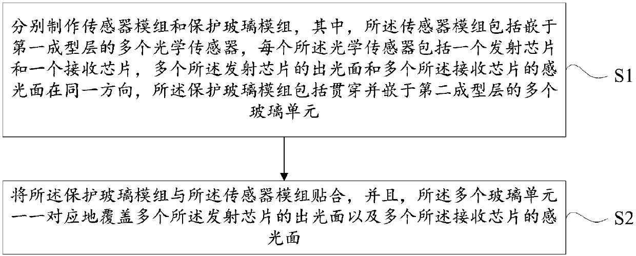
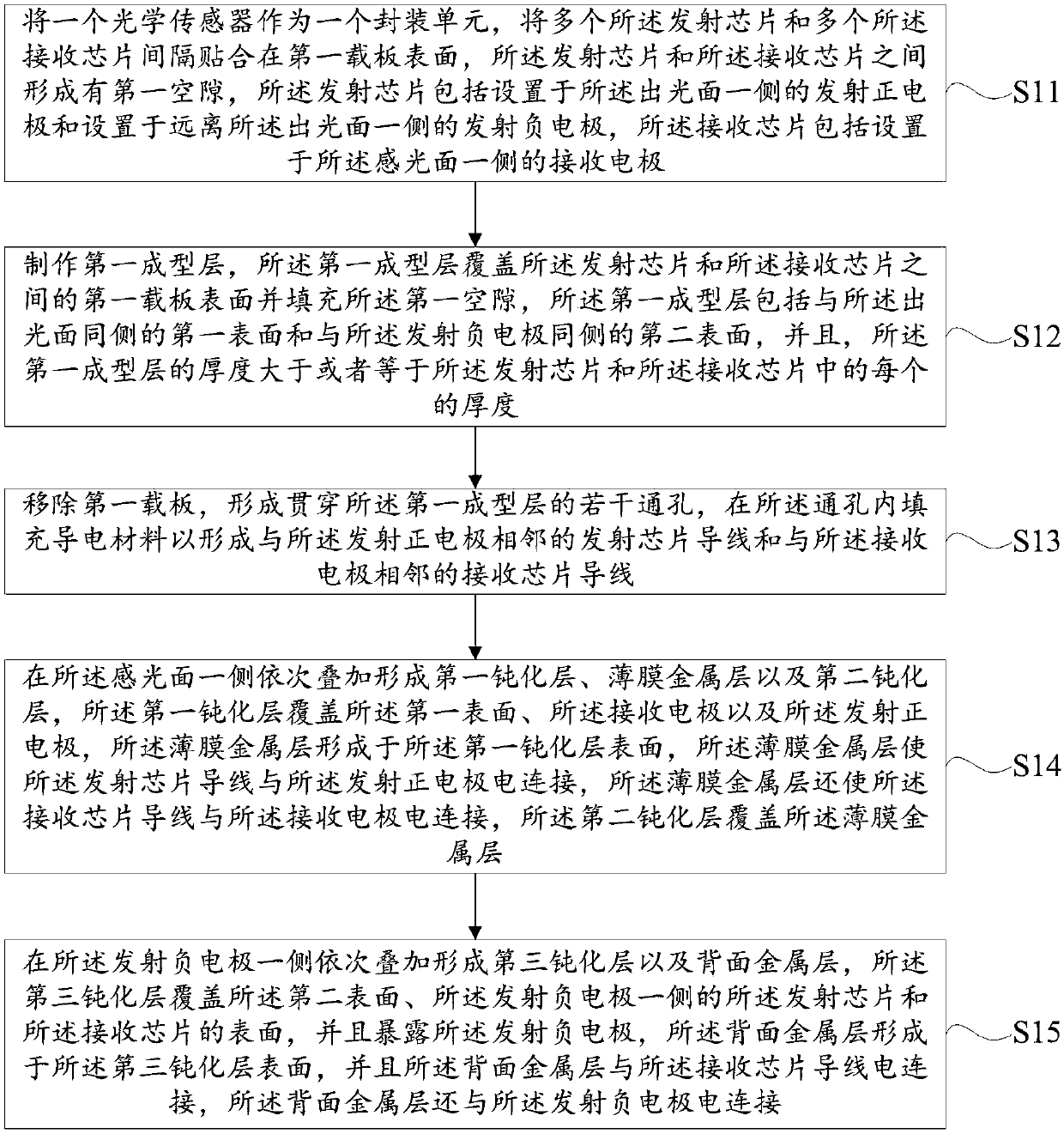
Examples
Embodiment Construction
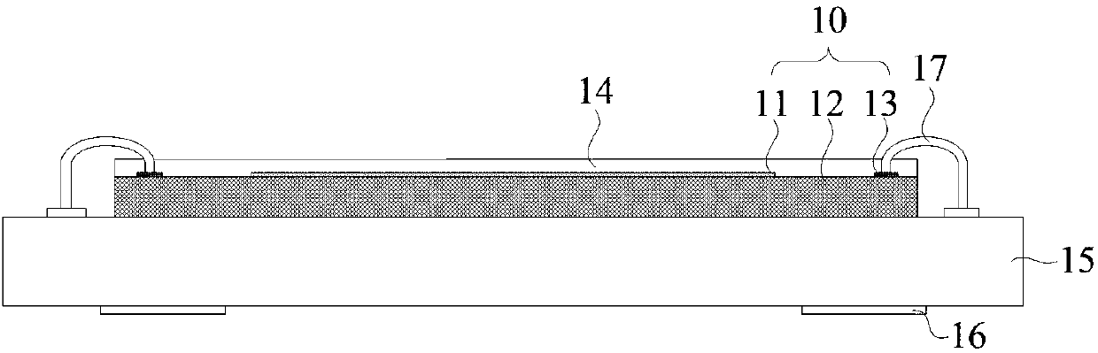
[0041] The packaging structure and packaging method of the optical sensor of the present invention will be further described in detail below in conjunction with the accompanying drawings and specific embodiments. According to the following description and accompanying drawings, the advantages and characteristics of the present invention will be clearer, however, it should be noted that the concept of the technical solution of the present invention can be implemented in many different forms, and is not limited to the specific implementation set forth herein. example. In addition, the drawings are all in a very simplified form and use imprecise scales, which are only used to facilitate and clearly assist the purpose of illustrating the embodiments of the present invention.
[0042] The terms "first", "second", etc. in the description and claims are used to distinguish between similar elements and not necessarily to describe a specific order or chronological order. It is to be u...
PUM
 Abstract
Description
Claims
Application Information