Display panel and manufacture method thereof

A technology for display panels and manufacturing methods, which is applied in semiconductor/solid-state device manufacturing, instruments, electrical components, etc., and can solve problems such as incomplete etching, a large amount of particles easily generated by the slotting process, and poor sensing, so as to improve reliability Effect

Active Publication Date: 2019-06-18
YUNGU GUAN TECH CO LTD
View PDF6 Cites 9 Cited by
  • Summary
  • Abstract
  • Description
  • Claims
  • Application Information

AI Technical Summary

Problems solved by technology

[0005] Flexible display devices usually adopt flexible OLED (Organic Light-Emitting Diode, organic light-emitting diode) devices, and flexible OLED devices are being widely used in smart terminal products such as mobile phones and tablet computers, because OLED devices are easy to customize appearance , more and more terminal manufacturers are applying it to full-screen and borderless products, and the way to form the mounting holes in the existing design is usually to use a knife wheel or laser cutting process on the display panel, along the line perpendicular to the lining The direction of the bottom substrate at least cuts off each film layer on the display panel, and cuts and grooves to form mounting holes for installing the hardware structure; but when the thickness of the array film layer is relatively large, it is extremely difficult to directly use laser cutting or knife wheel cutting technology. It is easy to cause damage to the organic light-emitting unit at the edge of the slotted area, resulting in abnormal display and poor sensing at the edge of the slotted area. When it is necessary to open large-diameter mounting holes on the array substrate, due to the limitation of dry etching equipment, it is impossible to directly etch the large-diameter mounting holes, and it is easy to cause incomplete etching.

Method used


Image

  • Display panel and manufacture method thereof
  • Display panel and manufacture method thereof
  • Display panel and manufacture method thereof

Examples


Embodiment Construction

[0032] The present invention will be described in detail below in conjunction with various embodiments shown in the drawings. However, these embodiments do not limit the present invention, and any structural, method, or functional changes made by those skilled in the art according to these embodiments are included in the protection scope of the present invention.

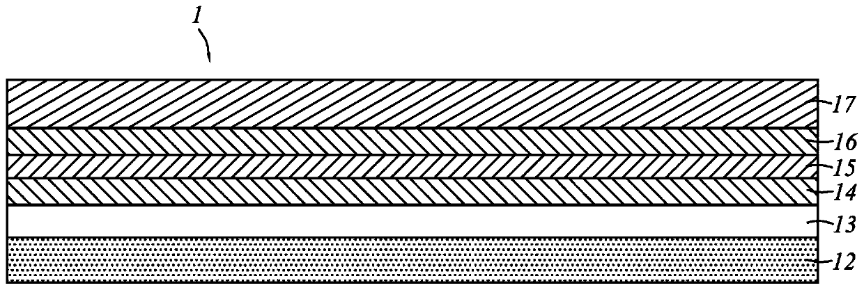
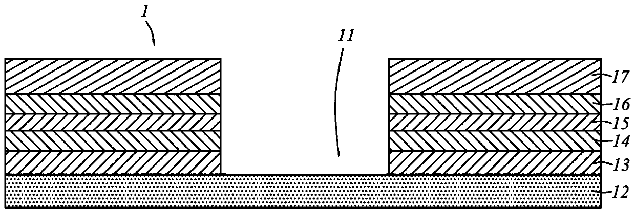
[0033] Please refer to Figure 1 to Figure 5 As shown, the display panel provided by the embodiment of the present invention is preferably a display panel with a full screen and no frame, and of course it can also be applied to an ordinary display panel with a frame or a narrow frame. The specific structure of the display panel is as follows and its preparation method are described in detail.

[0034] In the embodiment shown in the present invention, the display panel includes an array substrate 1 , an organic light-emitting layer formed on the upper surface of the array substrate 1 , and a packaging structure (not...


PUM


Abstract

The invention provides a display panel and a manufacture method thereof. The manufacture method of the display panel comprises steps of: providing an array substrate; reserving at least one pre-grooved area for forming an installation groove on the array substrate; forming a photoresist layer in the pre-grooved area; providing a mask plate with a designed pattern so as to block the array substrate, exposing and developing the pre-grooved area through the mask plate, so as to form at least one pre-etched area in the pre-grooved area; and grooving the pre-grooved area so as to form the installation groove. The display panel meets the requirement of etching on the array substrate so as to make a large-area installation groove, reduces particles in later grooving process and keeps the functional layer effective.

Description

technical field [0001] The present invention relates to the technical field of display panel manufacturing, in particular to a display panel and a manufacturing method thereof. Background technique [0002] Organic electroluminescent (OLED) devices have the characteristics of low power consumption, light weight, high brightness, wide field of view and fast response. In addition, one of the most attractive features of OLED devices is the ability to realize flexible display functions, making them widely used in portable Electronic equipment, wearable electronic equipment, vehicle electronic equipment and many other fields. [0003] In display devices such as mobile phones, tablet computers, etc., in order to realize the functions of Selfie, video call and fingerprint recognition, mounting holes are usually set in the non-display area outside the effective display area to install the front camera, earpiece, fingerprint, etc. Identify devices or physical buttons, etc., but this ...

Claims


Application Information

Patent Timeline
Patent Type & Authority Applications(China)
IPC IPC(8): H01L21/77H01L27/12H01L27/32G09F9/30
Inventor 王守坤
Owner YUNGU GUAN TECH CO LTD
Why Eureka
Try Eureka