Forming method for 3D NAND memory

A 3D NAND and memory technology, which is applied in the direction of electric solid-state devices, semiconductor devices, electrical components, etc., can solve problems such as storage structure failure, and achieve the effects of preventing failure, reducing etching difficulty, and preventing etching through or damage

Active Publication Date: 2019-06-18
YANGTZE MEMORY TECH CO LTD
View PDF7 Cites 7 Cited by
  • Summary
  • Abstract
  • Description
  • Claims
  • Application Information

AI Technical Summary

Problems solved by technology

[0004] In order to further increase the storage capacity, when forming the stack structure in the prior art, a multi-layer stack structure is usually formed, and each layer stack structure includes several alternatel...

Method used


Image

  • Forming method for 3D NAND memory
  • Forming method for 3D NAND memory
  • Forming method for 3D NAND memory

Examples


Embodiment Construction

[0030] As mentioned in the background, the existing multi-layer stacked 3D NAND memory has the problem of failure.

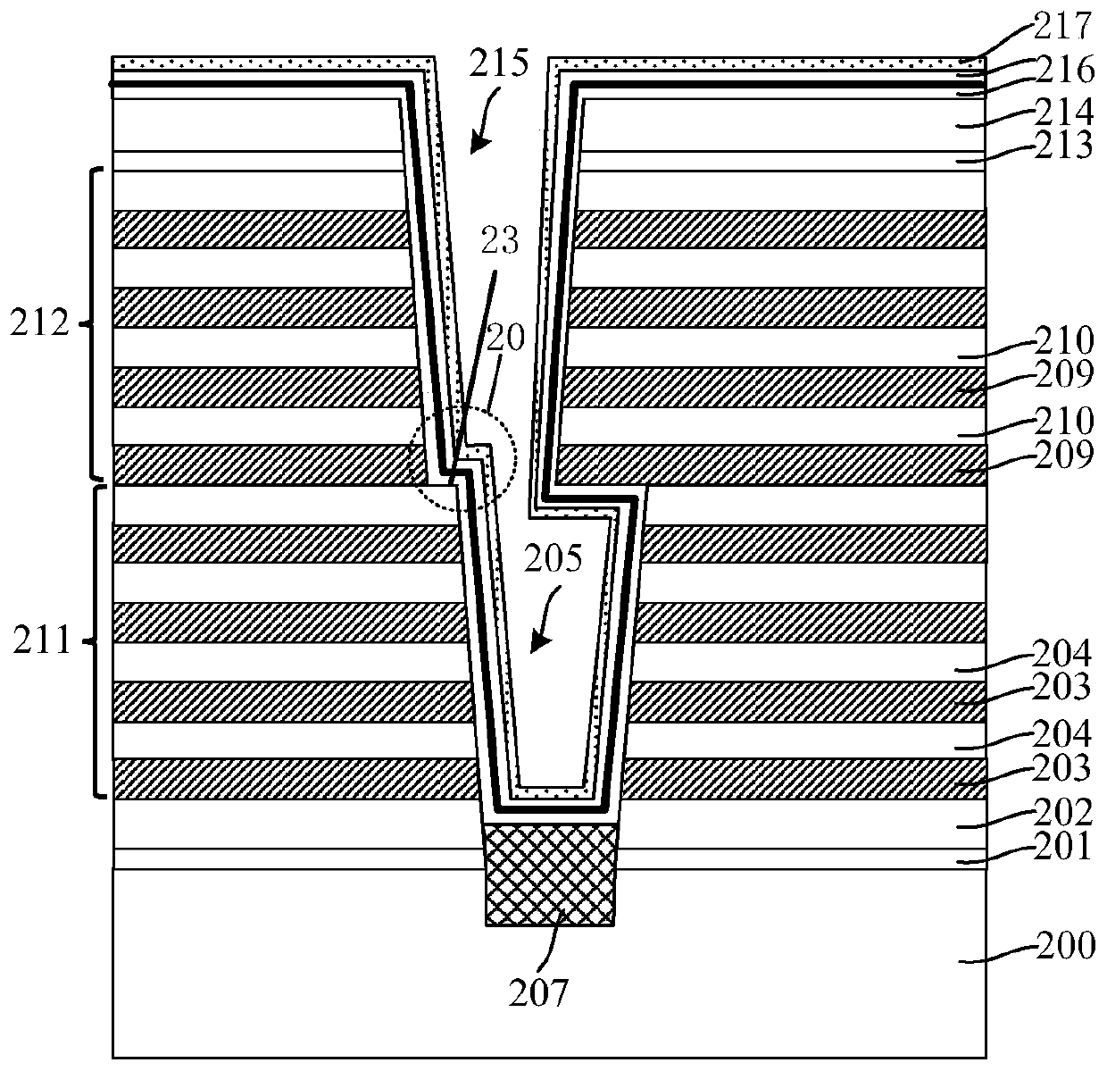
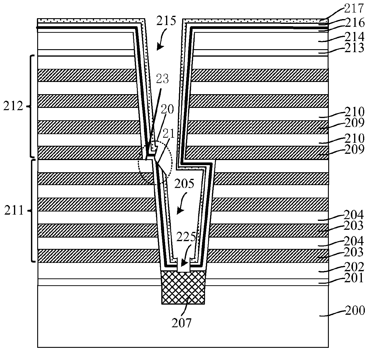
[0031] The study found that the location where the failure problem of multi-layer stacked 3D NAND memory generally occurs at the junction of the multi-layer stacked structure, please refer to figure 2 20 positions indicated by the dotted box in .

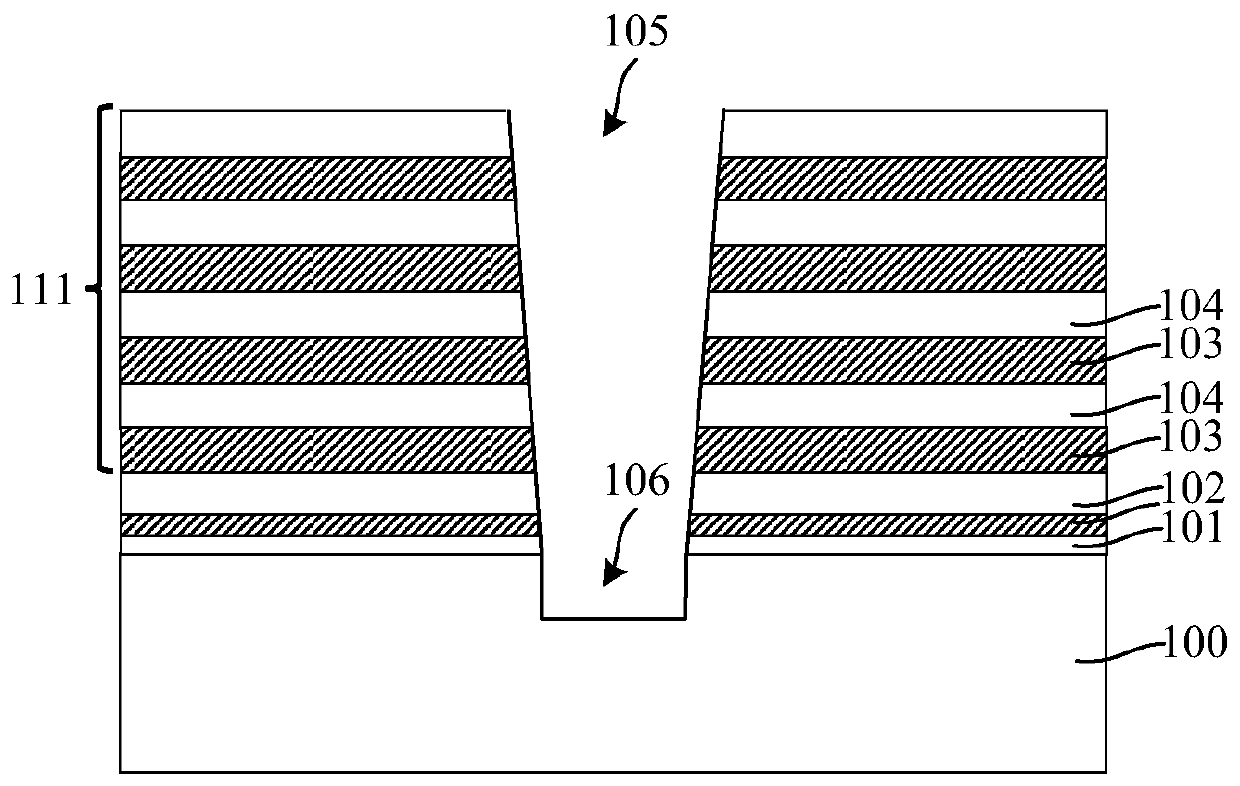
[0032] After further research, the specific reasons for the above problems are: Figure 1-2 It is a schematic diagram of the cross-sectional structure of the formation process of the 3D NAND memory according to an embodiment of the present invention. First, please refer to figure 1 , forming a first stack structure 211 on the semiconductor substrate 200, the first stack structure 211 includes a number of alternately stacked sacrificial layers 203 and insulating layers 204, the first stack structure 211 and the semiconductor substrate 200 can also be Form a buffer oxide layer 201 and a dielectric layer 202; etch th...


PUM


Abstract

A forming method for a 3D NAND memory comprises the following steps: providing a semiconductor substrate, wherein stack structures are formed on the semiconductor substrate, each stack structure comprises a plurality of sacrificial layers and a plurality of isolating layers which are alternately stacked, the stack structures are respectively provided with a first channel hole and a second channelhole which are communicated with each other, the second channel hole has an alignment offset relative to the first channel hole, a step is formed at the junction of the first channel hole and the second channel hole, and the first channel hole is filled with a sacrificial material layer; after a side wall is formed, carrying out etching-back to remove the sacrificial material layer with a part ofthe thickness; carrying out etching on the step, so that the gradient of the step is reduced; forming charge storage layers on the side walls and at the bottoms of the first channel hole and the second channel hole; forming channel hole sacrificial layers on the charge storage layers; and sequentially carrying out etching on the channel hole sacrificial layer and the charge storage layer at the bottom of the first channel hole, so that an opening is formed. The method provided by the invention has the advantages that the charge storage layer at the step can be prevented from being broken or damaged during the etching, so that failure of the memory can be avoided.

Description

technical field [0001] The invention relates to the field of semiconductor manufacturing, in particular to a method for forming a 3D NAND memory. Background technique [0002] NAND flash memory is a better storage device than hard disk drives, and it has been widely used in electronic products as people pursue non-volatile storage products with low power consumption, light weight and high performance. At present, the NAND flash memory with a planar structure is close to the limit of practical expansion. In order to further increase the storage capacity and reduce the storage cost per bit, a 3D NAND memory with a 3D structure is proposed. [0003] The manufacturing process of the existing 3D NAND memory includes: providing a substrate on which a stacked structure in which isolation layers and sacrificial layers are alternately stacked; etching the stacked structure to form an exposed substrate surface in the stacked structure channel hole; form a storage structure in the cha...

Claims


Application Information

Patent Timeline
IPC IPC(8): H01L27/1157H01L27/11582
Inventor 霍宗亮薛家倩
Owner YANGTZE MEMORY TECH CO LTD
Why Eureka
Try Eureka