Micro-nano device

A device and micro-nano technology, applied in the direction of nanotechnology, nanotechnology, nanotechnology for materials and surface science, etc., can solve problems such as increased workload, difficulty in obtaining accurate qualitative or quantitative signals, and increased work costs , to achieve the effects of wide matching range, strong universality, reduced workload and cost

Active Publication Date: 2019-06-21
苏州英菲尼纳米科技有限公司
View PDF2 Cites 0 Cited by
  • Summary
  • Abstract
  • Description
  • Claims
  • Application Information

AI Technical Summary

Problems solved by technology

[0003] At present, the direction of research on micro-nano devices is basically to maintain uniformity and prepare controllable and repeatable micro-nano devices. However, in practical applications, such as catalysis or detection, it is difficult to use when it needs to act on multiple substances. It can be realized by a single micro-nano device (nanomaterials with a single particle size may only have a significant catalytic effect on a specific substance). If you don’t know what kind of substance you need to detect, you may need to try one by one, which will undoubtedly increase the workload and increase the work cost, especially in the field of SERS (Surface Enhanced Raman Scattering) detection. The big difficulty is that the samples to be tested require complicated pre-treatment, otherwise the samples to be tested have many interfering substances, and it is difficult to obtain accurate qualitative or quantitative signals

Method used


Image

  • Micro-nano device
  • Micro-nano device
  • Micro-nano device

Examples


Embodiment 1

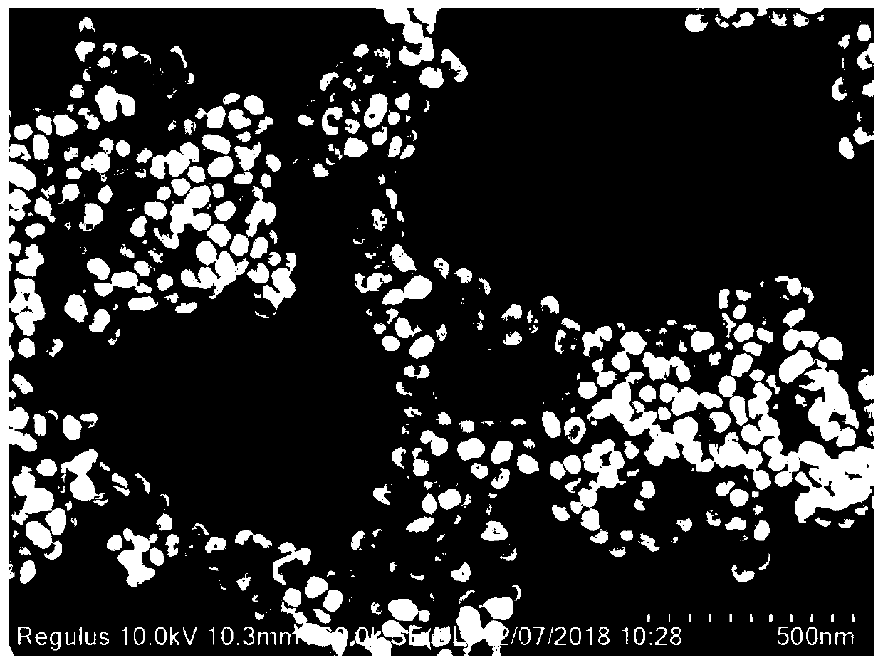
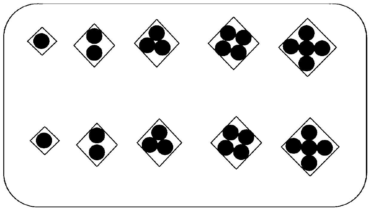
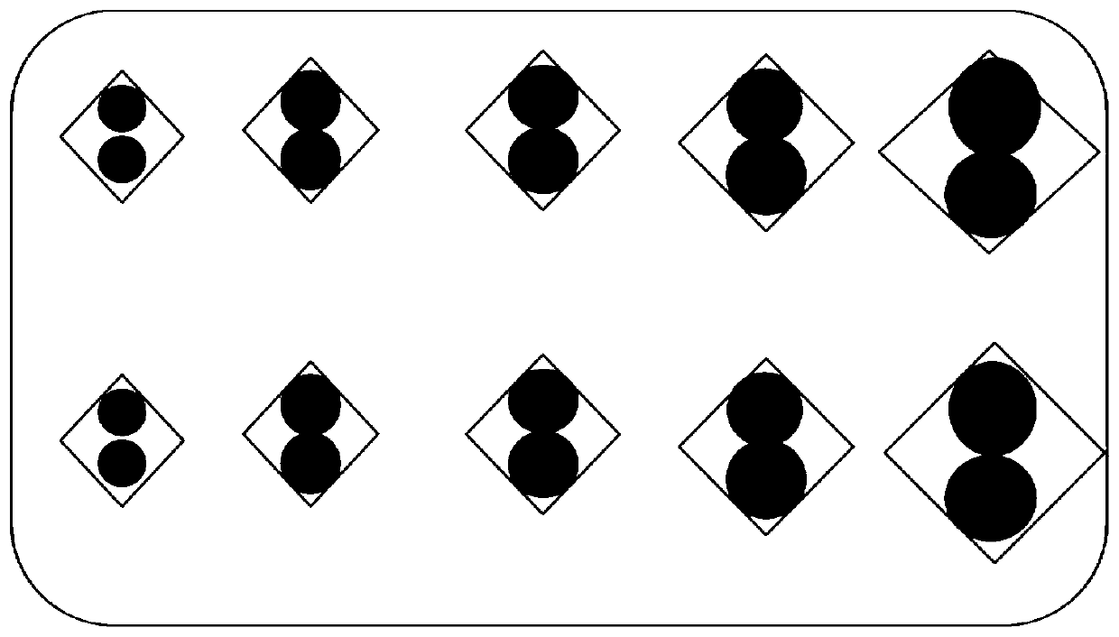
[0044] A micro-nano device for SERS detection, comprising a substrate and a first module, a second module, a third module, and a fourth module bonded on the substrate. The first module includes a substrate and nanoparticle aggregates bonded on the substrate. The substrate is provided with multiple pits, the average size of the pits is about 500nm, and the pits self-assembled with nanoparticle aggregates and nanoparticle aggregates. It is composed of three silver nanoparticles with a particle diameter of about 40 nm, and the average size of the nanoparticle aggregate is about 120 nm. The second module is basically the same as the first module. The difference is that the average size of the nanoparticle aggregate of the second module is about 200nm, which is composed of 5 silver nanoparticles with a particle size of about 40nm. The third module is basically the same as the second module, except that the average size of the nanoparticle aggregate is 280nm, which is composed of 7 s...

Embodiment 2

[0046] It is basically the same as in Example 1, except that the size of the silver nanoparticles is 60 nm.

Embodiment 3

[0048] It is basically the same as in Example 1, except that the size of the silver nanoparticles is 100 nm.


PUM

PropertyMeasurementUnit
sizeaaaaaaaaaa
sizeaaaaaaaaaa
thicknessaaaaaaaaaa

Abstract

The invention discloses a micro-nano device. The device includes multiple modules, each of the modules comprises a substrate having a plurality of concave pits and nanoparticle aggregates self-assembled in the concave pits, and the average size of the nanoparticle aggregates in the different modules is different; and the micro-nano device of the invention has the characteristics of simultaneouslyperforming functions such as detection, catalysis and degradation on a plurality of substances, and has the advantages of wide matching range and strong universality.

Description

Technical field [0001] The invention belongs to the field of micro-nano functional devices, and specifically relates to a micro-nano device. Background technique [0002] At the micro-nano scale, the properties of materials will change drastically. Although the mechanical theory of the macroscopic world has been fully developed, there is no mature theoretical system to describe the mechanical properties and internal mechanisms of micro-nano-scale materials. . And some special micro-nano structure devices have unique catalytic and photoelectric properties, which make a large number of researchers to study. [0003] At present, the research direction of micro-nano devices is basically to maintain uniformity and prepare controllable and reproducible micro-nano devices. However, in practical applications, such as catalysis or detection, it is difficult to use when it has an effect on multiple substances. A single micro-nano device (a single particle size nanomaterial may only have a ...

Claims


Application Information

Patent Timeline
Patent Type & Authority Applications(China)
IPC IPC(8): G01N21/65B82Y30/00B82Y40/00
Inventor 孙海龙郭清华马从乔李大飞
Owner 苏州英菲尼纳米科技有限公司
Why Eureka
Try Eureka