Unlock instant, AI-driven research and patent intelligence for your innovation.

Array substrate, manufacturing method thereof, liquid crystal display device and driving method

An array substrate and color filter substrate technology, which is applied in the field of liquid crystal display, can solve the problems of difficulty in making breakthrough improvements in afterimage improvement effect, and cannot guarantee that no ion impurities will be introduced, so as to increase the privacy protection effect and improve the coupling effect. , the effect of improving the aggregation state

Active Publication Date: 2019-06-21
KUSN INFOVISION OPTOELECTRONICS
View PDF5 Cites 0 Cited by
  • Summary
  • Abstract
  • Description
  • Claims
  • Application Information

AI Technical Summary

Problems solved by technology

However, it is currently impossible to find a liquid crystal that does not contain ionic impurities, nor can it guarantee that ionic impurities will not be introduced during the manufacturing process. It is difficult to make a breakthrough improvement in the improvement effect of the afterimage from the raw material surface and the manufacturing process.

Method used


Image

  • Array substrate, manufacturing method thereof, liquid crystal display device and driving method
  • Array substrate, manufacturing method thereof, liquid crystal display device and driving method
  • Array substrate, manufacturing method thereof, liquid crystal display device and driving method

Examples


no. 1 example

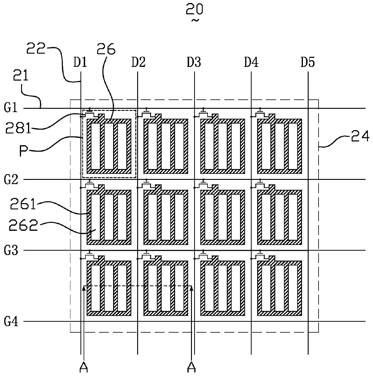
[0044] Please refer to Figure 1 to Figure 2 The first embodiment of the present invention provides an array substrate 20 , including a transparent substrate 23 and a common electrode 24 , an insulating layer 25 , a pixel electrode 26 and an alignment layer 27 sequentially disposed on the transparent substrate 23 . On the array substrate 20, a plurality of pixel units P are defined by a plurality of scanning lines 21 and a plurality of data lines 22 insulated from each other, and a pixel electrode 26 is arranged in each pixel unit P, and the pixel electrode 26 passes through a first thin film transistor (TFT) 281 is connected to the scan line 21 and the data line 22 adjacent to the first thin film transistor 281 .

[0045] The pixel electrode 26 is a comb-shaped structure having first electrode strips 261 and first slits 262, and the rest of the insulating layer 25 is etched and thinned except for the position corresponding to the first electrode strip 261 of each pixel electr...

no. 2 example

[0052] Please refer to Figure 5 to Figure 7 The second embodiment of the present invention provides an array substrate 20 , including a transparent substrate 23 and a common electrode 24 , an insulating layer 25 , a pixel electrode 26 and an alignment layer 27 sequentially disposed on the transparent substrate 23 . The array substrate 20 is defined by a plurality of scanning lines 21 and a plurality of data lines 22 insulated from each other to form a plurality of pixel units P, and a pixel electrode 26 is arranged in each pixel unit P, and the pixel electrode 26 passes through a first thin film transistor (TFT) 281 It is connected to the scan line 21 and the data line 22 adjacent to the first thin film transistor 281 .

[0053] A plurality of common lines 29 are also provided on the array substrate 20, and the plurality of common lines 29 extend in the same direction as the plurality of data lines 22, and each of the plurality of data lines 22 arranged side by side forms a p...

no. 3 example

[0062] Please refer to Figure 10a to Figure 10e , the third embodiment of the present invention provides a method for manufacturing the above-mentioned array substrate 20, including steps:

[0063] Please refer to Figure 10a , after forming the TFT array on the transparent substrate 23, deposit the first transparent conductive layer on the TFT array, and etch and pattern the first transparent conductive layer to form the common electrode 24; wherein the transparent substrate 23 can be a glass substrate Or a plastic substrate. Fabrication of a TFT array on the transparent substrate 23 is well known to those skilled in the art, and will not be repeated here.

[0064] Please refer to Figure 10b , depositing an insulating layer 25 on the common electrode 24; wherein, the insulating layer 25 is, for example, silicon oxide (SiOx), silicon nitride (SiNx), or silicon oxynitride (SiONx).

[0065] Please refer to Figure 10c , depositing a second transparent conductive layer on t...


PUM


Abstract

An array substrate, a manufacturing method thereof, a liquid crystal display device and a driving method are disclosed. The array substrate comprises a common electrode, an insulating layer, pixel electrodes and an alignment layer which are sequentially disposed on a transparent substrate, wherein each pixel electrode is a comb-like structure having a first electrode strip and a first slit; the areas, except positions corresponding to the first electrode strip of each of the pixel electrodes, of the insulating layer are etched and thinned, and recesses are formed at the thinned positions; theinsulating layer is provided with ridges at the positions corresponding to the first electrode strip of each of the pixel electrodes; and the first electrode strip of each pixel electrode covers the ridge of the insulating layer. The alignment layer formed in the array substrate is close to the common electrode and is fully in contact with the common electrode in order to improve the influence ofthe voltage switching to the common electrode on the pixel electrode, improve the coupling effect of the electrodes, and improve the aggregation states of the ions in the liquid crystal, thereby improving an afterimage problem, and improving the anti-spying effect of the liquid crystal display device at a narrow viewing angle.

Description

technical field [0001] The invention relates to the technical field of liquid crystal display, in particular to an array substrate and a manufacturing method, a liquid crystal display device and a driving method. Background technique [0002] Liquid crystal display (liquid crystal display, LCD) has the advantages of good image quality, small size, light weight, low driving voltage, low power consumption, no radiation and relatively low manufacturing cost, and occupies a dominant position in the field of flat panel display. [0003] In the early days, most LCDs used TN (Twisted Nematic, twisted nematic) mode, and the pixel electrode and common electrode of the TN type liquid crystal display device were respectively formed on the upper and lower substrates, and the viewing angle range was relatively small. In order to solve the viewing angle problem, the industry has proposed liquid crystal display devices with wide viewing angle technologies such as IPS (In-Plane Switching) m...

Claims


Application Information

Patent Timeline
Patent Type & Authority Applications(China)
IPC IPC(8): G02F1/13G02F1/133G02F1/1343G02F1/1345G02F1/1362G02F1/1337
Inventor 梁文龙刘晓杏刘洪海
Owner KUSN INFOVISION OPTOELECTRONICS