Integrated circuit chip photoresist removing device and process

A photoresist removal and integrated circuit technology, applied in the processing of photosensitive materials, etc., can solve the problems of consumption, excessive degumming cost, turbulent flow, etc., to improve the removal efficiency and reduce the residual defect rate.

Pending Publication Date: 2019-06-28
JIANGSU UNION SEMICON
View PDF1 Cites 0 Cited by
  • Summary
  • Abstract
  • Description
  • Claims
  • Application Information

AI Technical Summary

Problems solved by technology

This method achieves the effect of thorough degumming by soaking in the photoresist solution for a sufficient time and assisting certain plasma cleaning; but its disadvantages are that the whole process takes a long time, is inefficient, and consumes a lot of degumming costs.
[0004] In the integrated circuit chip manufacturing industry, photoresist removal liquid is usually used to remove the photoresist on the surface of the wafer. This reaction uses the mechanism of "photoresist swelling + photoresist stripping + photoresist dissolution". Ultrasonic devices are added in the process to accelerate the photoresist removal reaction; but the disadvantage of this process is that because of the cavitation effect of ultrasound, a large number of jets with bubbles will be formed in the photoresist solution, and finally there will be eddy currents in the photoresist solution , Turbulent flow is generated, when the ultrasonic is normally turned on, part of the undissolved photoresist remains in the photoresist removal solution, and the photoresist cannot be removed, so it is easy for the undissolved photoresist to stick back to the chip, forming photoresist residue, Ultimately lead to loss of chip yield

Method used


Image

  • Integrated circuit chip photoresist removing device and process
  • Integrated circuit chip photoresist removing device and process
  • Integrated circuit chip photoresist removing device and process

Examples


Embodiment 1

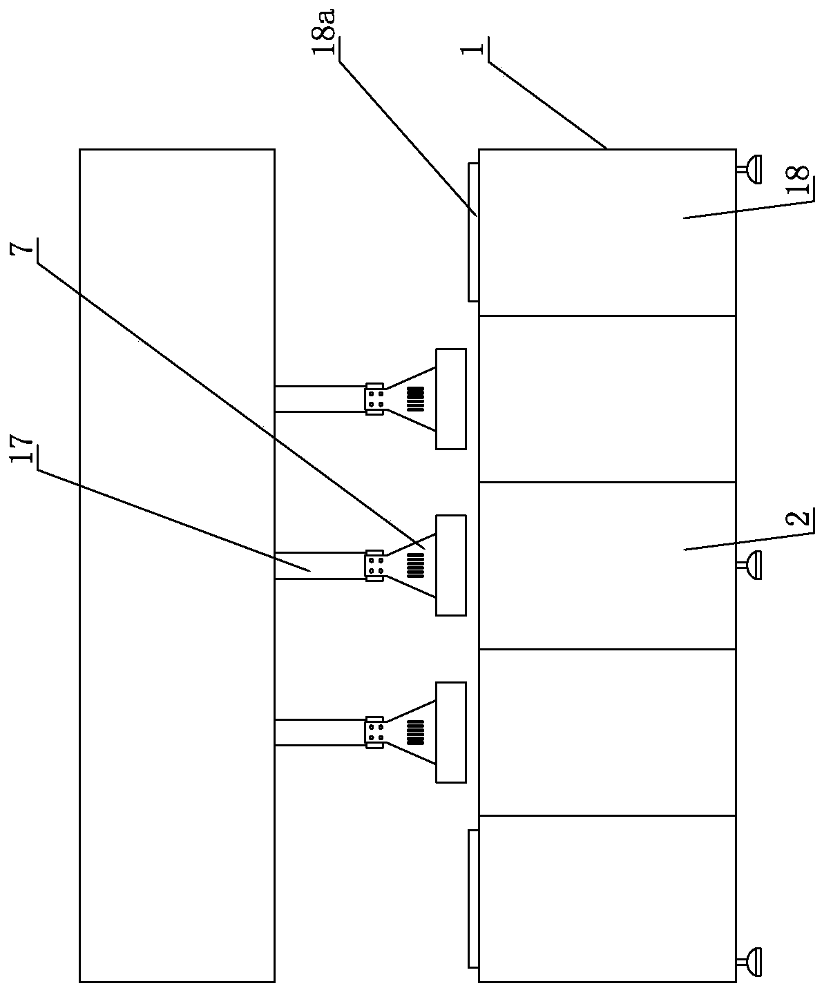
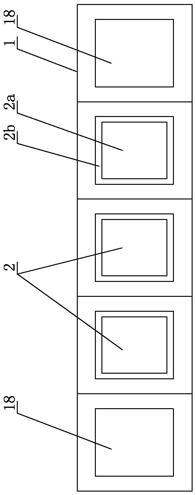
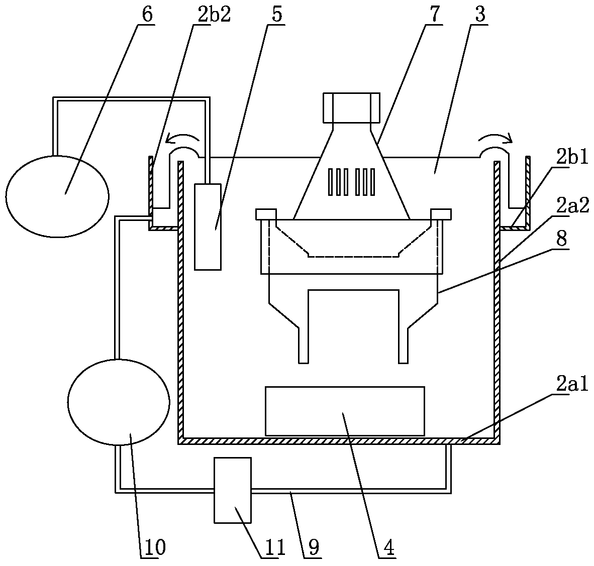
[0037] Such as Figure 1-11 , is a photoresist removing device for an integrated circuit chip, comprising a machine 1, on which a plurality of photoresist removing tanks 2 are arranged in sequence, and each photoresist removing tank 2 includes an inner tank 2a and an outer tank body 2b, the outer tank body 2b is located on the outer periphery of the inner tank body 2a, and the inner tank body 2a is filled with a photoresist removal liquid 3 that can overflow into the outer tank body 2b, and the main formula of the photoresist removal liquid 3 is "nitromethylpyrrolidone , sulfones (such as dimethyl sulfoxide), alcohols (2-aminoethanol), amines (such as ethanolamine), alkalis (such as tetramethylammonium hydroxide)" one or more of them; An ultrasonic generator 4 is arranged in the tank body 2a, and a heating device 5 is also arranged in the inner tank body 2a. The heating device 5 is electrically connected to the temperature control system 6, and a liftable wafer carrier 7 is pl...

Embodiment 2

[0049] Such as Figure 1-11 , is a photoresist removing device for an integrated circuit chip, comprising a machine 1, on which a plurality of photoresist removing tanks 2 are arranged in sequence, and each photoresist removing tank 2 includes an inner tank 2a and an outer tank body 2b, the outer tank body 2b is located on the outer periphery of the inner tank body 2a, the inner tank body 2a contains a photoresist liquid 3 that can overflow into the outer tank body 2b, the inner tank body 2a is provided with an ultrasonic generator 4, and the inner tank body 2a A heating device 5 is also provided in the tank body 2a, and the heating device 5 is electrically connected to the temperature control system 6. A liftable wafer carrier 7 is placed in the inner tank body 2a, and a wafer boat 8 is positioned on the wafer carrier 7 , a number of parallel wafers are vertically placed in the crystal boat 8; the outer tank 2b is connected to the bottom of the inner tank 2a through an extern...

Embodiment 3

[0060] Such as Figure 1-11 , is a photoresist removing device for an integrated circuit chip, comprising a machine 1, on which a plurality of photoresist removing tanks 2 are arranged in sequence, and each photoresist removing tank 2 includes an inner tank 2a and an outer tank body 2b, the outer tank body 2b is located on the outer periphery of the inner tank body 2a, the inner tank body 2a contains a photoresist liquid 3 that can overflow into the outer tank body 2b, the inner tank body 2a is provided with an ultrasonic generator 4, and the inner tank body 2a A heating device 5 is also provided in the tank body 2a, and the heating device 5 is electrically connected to the temperature control system 6. A liftable wafer carrier 7 is placed in the inner tank body 2a, and a wafer boat 8 is positioned on the wafer carrier 7 , a number of parallel wafers are vertically placed in the crystal boat 8; the outer tank 2b is connected to the bottom of the inner tank 2a through an extern...


PUM


Abstract

The invention discloses an integrated circuit chip photoresist removing device and process in the field of a semiconductor integrated circuit. The device comprises a machine table. A plurality of photoresist removing groove bodies are arranged in order on the machine table, ultrasonic generators are arranged in inner groove bodies, heating devices are arranged in the inner groove bodies, wafer carriers capable of going up and down are placed in the inner groove bodies, wafer boats are placed on the wafer carriers, and the insides of outer groove bodies are connected to the bottoms of the innergroove bodies through external pipelines. The process includes a step of placing a wafer into each wafer groove of each wafer boat, a step of placing each wafer boat on a wafer carrier, a step of allowing a control rod to drive each wafer boat to go down to be submerged into a photoresist groove body, a step of allowing a circulation pump to work, at the same time, turning on the ultrasonic generators to work for N seconds, and then turning off the ultrasonic generators for N seconds, a step of repeating the above steps for M times, a step of put the wafer boats into a washing tank to wash off the photoresist on the wafers. According to the invention, the photoresist on the wafers can be removed, the photoresist is prevented from being stuck back to the wafers, and the photoresist removalefficiency is improved.

Description

technical field [0001] The invention belongs to the field of semiconductor integrated circuits, in particular to a photoresist removal device and process for integrated circuit chips. Background technique [0002] In the prior art, in the entire manufacturing process of integrated circuit chips, the production of transparent electrodes and metal electrode patterns is often completed with photoresist, and the removal of photoresist after completing the electrodes inevitably becomes a part of the integrated circuit chip manufacturing process. an important link. [0003] In the prior art, there is a method for effectively removing photoresist, its patent application number: 201510147639.7; application date: 2015-03-31; publication number: 104882364A; publication date: 2015-09-02; the method is implemented according to the following steps : Step 1: Soak the wafer to be removed in the photoresist removal solution for 30-60 minutes; Step 2: Take out the photoresist removal soluti...

Claims


Application Information

Patent Timeline
Patent Type & Authority Applications(China)
IPC IPC(8): G03F7/42
Inventor 时庆楠周德榕郑忠张伟李文浩谢巍
Owner JIANGSU UNION SEMICON
Why Eureka
Try Eureka