Semiconductor packaging method

A packaging method and semiconductor technology, applied in the fields of semiconductor devices, semiconductor/solid-state device manufacturing, electric solid-state devices, etc., can solve the problems of short circuit, product failure, low production yield, etc., to improve yield, improve product quality, eliminate The effect of the short circuit problem

Inactive Publication Date: 2019-06-28
嘉盛半导体(苏州)有限公司
View PDF4 Cites 3 Cited by
  • Summary
  • Abstract
  • Description
  • Claims
  • Application Information

AI Technical Summary

Problems solved by technology

This will cause a bridge between the pins of the final semiconductor package unit, resulting in a short circuit, resulting in product failure and low production yield

Method used


Image

  • Semiconductor packaging method
  • Semiconductor packaging method
  • Semiconductor packaging method

Examples


Embodiment Construction

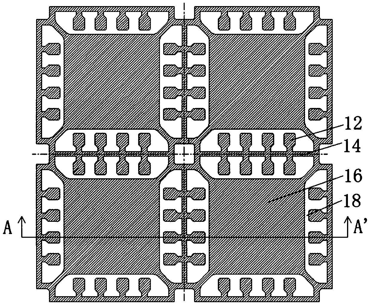
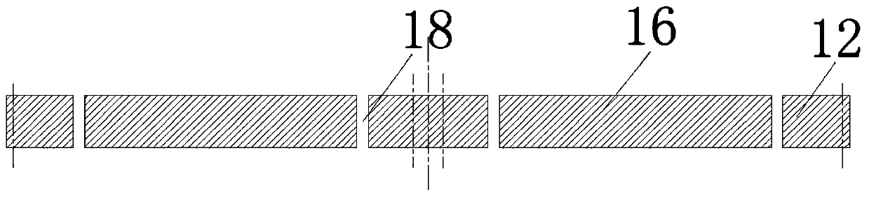
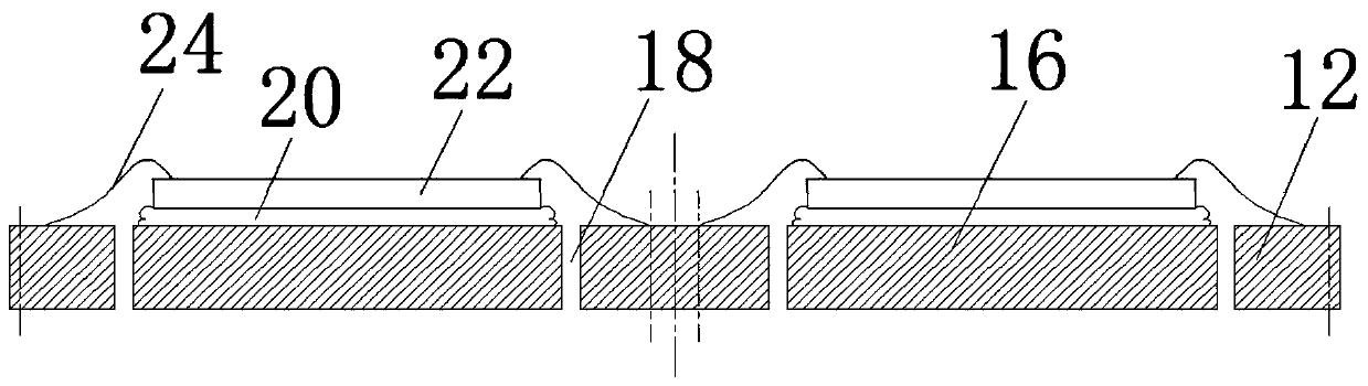
[0069] In order to make those skilled in the art better understand the technical solutions of the present invention, the technical solutions in the embodiments of the present invention will be clearly and completely described below with reference to the accompanying drawings in the embodiments of the present invention. Obviously, the described The embodiments are only some of the embodiments of the present invention, but not all of the embodiments. Based on the embodiments of the present invention, all other embodiments obtained by persons of ordinary skill in the art without creative work shall fall within the protection scope of the present invention.

[0070] It should be noted that when an element is referred to as being "disposed on" another element, it can be directly on the other element or intervening another element may also be present. When an element is referred to as being "connected" to another element, it can be directly connected to the other element or it may b...


PUM


Abstract

The invention discloses a semiconductor packaging method comprising the steps of: providing a metal substrate, wherein the metal substrate has opposite front and back sides, the metal substrate comprises a plurality of operating units, each operating unit comprises pins, and the pins of two adjacent operating units are connected through a scribe line connecting strip; pasting and electrically connecting a semiconductor chip; fixing the semiconductor chip to the front side of the metal substrate, and electrically connecting the pins to the semiconductor chip; performing plastic package; forminga plastic package layer on the front side of the metal substrate, wherein the plastic package layer completely covers the semiconductor chip and the front side of the metal substrate; performing halfcutting; cutting the scribe line connecting strip on the back side of the metal substrate to form a groove, wherein the adjacent operating units are still in a conductive interconnection state afterthe half cutting, and the scribe line connecting strip generates metal burrs in the half cutting process; removing the metal burrs; forming a first protective layer; and performing full cutting. The semiconductor packaging method provided by the application can remove metal debris or wire residues formed in the cutting step.

Description

technical field [0001] The present application relates to the technical field of semiconductor packaging, and in particular, to a semiconductor packaging method. Background technique [0002] The descriptions in this section merely provide background information related to the present disclosure and do not constitute prior art. [0003] In order to meet the higher performance requirements of semiconductor packaging products in some industries (such as automotive electronic products), it is necessary to form a protective layer on the sides of the semiconductor packaging product pins to prevent oxidation of the pin sides, so as to improve the performance of semiconductor packaging products. Reliability and solderability when connecting to other components. [0004] Announcement No. CN204834611U provides a known embodiment that can form an anti-oxidation protective layer on the side of a lead of a semiconductor package product. The specific implementation process of the known ...

Claims


Application Information

Patent Timeline
IPC IPC(8): H01L21/56H01L21/78
CPCH01L2224/16245H01L2224/32245H01L2224/48247H01L2224/73265H01L2224/97H01L2924/181H01L2924/00012H01L2924/00
Inventor 朱健荣王健王超石岩
Owner 嘉盛半导体(苏州)有限公司
Why Eureka
Try Eureka