Touch electrode structure, touch substrate and manufacturing method, display panel and device

A technology of touch electrodes and conductive structures, applied in circuits, electrical components, electric solid devices, etc., can solve problems such as uneven touch electrode signals, achieve improved touch effects, low resistance, and strong signal transmission capabilities Effect

Active Publication Date: 2021-03-16
BOE TECH GRP CO LTD +1
View PDF7 Cites 0 Cited by
  • Summary
  • Abstract
  • Description
  • Claims
  • Application Information

AI Technical Summary

Problems solved by technology

[0004] The present invention at least partly solves the problem of uneven signals at different positions of the touch electrodes in the existing touch substrate, and provides a touch electrode structure that can ensure the uniformity of the internal signals of the touch electrodes, a touch substrate and a preparation method, and a display panel and devices

Method used


Image

  • Touch electrode structure, touch substrate and manufacturing method, display panel and device
  • Touch electrode structure, touch substrate and manufacturing method, display panel and device
  • Touch electrode structure, touch substrate and manufacturing method, display panel and device

Examples


Embodiment 1

[0057] This embodiment provides a touch electrode structure, which includes:

[0058] Touch electrodes made of transparent conductive materials;

[0059] A signal line corresponding to the touch electrode, at least one insulating layer is provided between the signal line and the touch electrode;

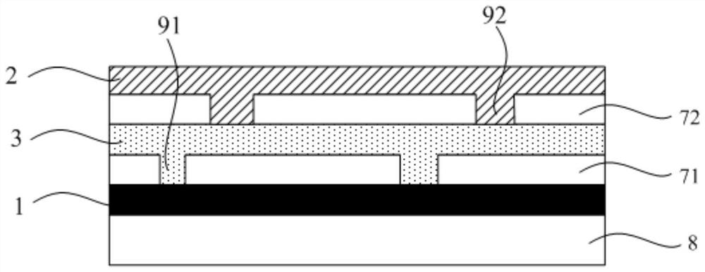
[0060] An auxiliary conductive structure made of metal, the auxiliary conductive structure is connected to the touch electrode at multiple positions; and a first insulating layer is provided between the auxiliary conductive structure and the signal line, and the first via hole in the first insulating layer is connected to the touch The signal line corresponding to the control electrode is connected.

[0061] In the touch electrode structure of this embodiment, the signal line is indirectly electrically connected to the touch electrode through the auxiliary conductive structure, and the auxiliary conductive structure is made of metal, which has low resistance and strong signal transm...

Embodiment 2

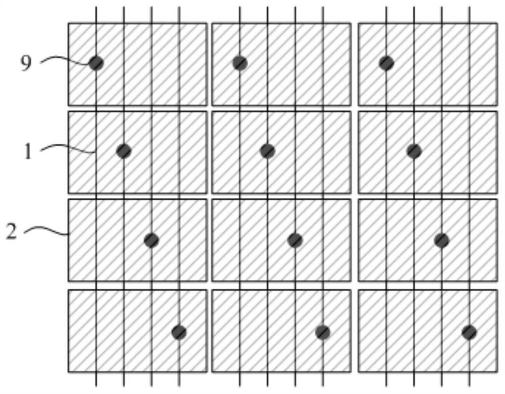
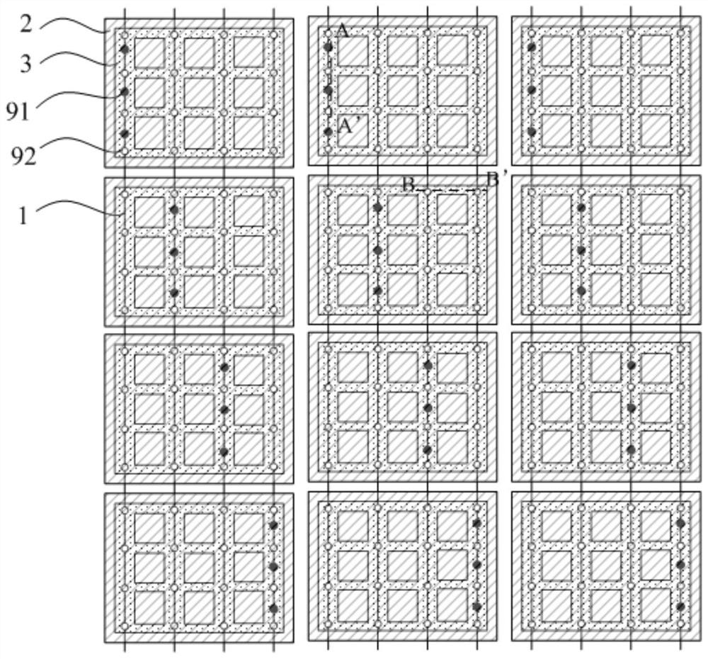
[0072] Such as Figure 2 to Figure 5 As shown, the present embodiment provides a touch control substrate, which includes the above touch control electrode structure. Specifically, the touch substrate includes:

[0073] A plurality of touch electrodes 2 arranged at intervals and made of transparent conductive materials;

[0074] A plurality of signal lines 1 correspond one-to-one to the touch electrodes 2 , and at least one insulating layer (such as a first insulating layer 71 , a second insulating layer 72 , etc.) is disposed between the signal lines 1 and the touch electrodes 2 .

[0075] The touch substrate of this embodiment is used to realize the touch function, that is, to identify the touched position. In the touch substrate, a plurality of touch electrodes 2 made of transparent conductive materials such as indium tin oxide (ITO) are arranged at intervals, and each touch electrode 2 corresponds to a signal line 1 . Thus, a touch signal (such as a high-frequency signal...

Embodiment 3

[0105] This embodiment provides a method for preparing the above-mentioned touch substrate, which includes:

[0106] A step of forming a touch electrode, a step of forming a signal line, a step of forming a first insulating layer, and a step of forming an auxiliary conductive structure.

[0107] That is to say, the manufacturing method of the touch control substrate in this embodiment includes the steps of forming each structure in the above touch control substrate.

[0108] It should be understood that when the touch control substrate includes other structures such as gate lines and data lines, the preparation method also includes the step of forming these structures, and these structures can be formed separately or synchronously with the above touch control structures. of.

[0109] Wherein, the formation of the above structures can be realized by conventional techniques such as patterning technology; and the order of forming each structure is determined by the stacking orde...


PUM


Abstract

The invention provides a touch electrode structure, a touch substrate and a preparation method thereof, a display panel, and a display device, belonging to the field of touch technology, which can at least partly solve the uneven signal at different positions of the touch electrode in the existing touch substrate The problem. The touch electrode structure of the present invention includes: a touch electrode made of transparent conductive material; a signal line corresponding to the touch electrode, at least one insulating layer is arranged between the signal line and the touch electrode; A conductive structure, the auxiliary conductive structure is connected to the touch electrode at multiple positions; and a first insulating layer is provided between the auxiliary conductive structure and the signal line, and the touch sensor is connected to the first via hole in the first insulating layer. The signal line corresponding to the electrode is connected.

Description

technical field [0001] The invention belongs to the field of touch technology, and in particular relates to a touch electrode structure, a touch substrate and a preparation method, a display panel and a device. Background technique [0002] Such as figure 1 As shown, the existing self-capacitive touch substrate includes a plurality of touch electrodes 2 arranged at intervals (such as figure 1 As shown in the plurality of electrode blocks arranged in an array), each touch electrode 2 is correspondingly provided with a signal line 1 for transmitting signals thereto. An insulating layer is provided between the touch electrodes 2 and the signal lines 1 , and the corresponding touch electrodes 2 and the signal lines 1 are connected through via holes 9 in the insulating layer. [0003] In order not to affect the display, the touch electrode 2 is made of transparent conductive materials such as indium tin oxide (ITO), which has a large resistance, and the signal has a large delay...

Claims


Application Information

Patent Timeline
Patent Type & Authority Patents(China)
IPC IPC(8): G02F1/1343G02F1/1333G06F3/044G06F3/041
CPCG02F1/134309G02F1/13338G06F3/044G06F3/0416G06F3/0412G06F2203/04111G06F2203/04103G02F1/1333G02F1/1343G06F3/041G06F3/04164H01L27/1255
Inventor 胡伟频魏从从王纯姜明宵孙晓
Owner BOE TECH GRP CO LTD
Why Eureka
Try Eureka