Silicon carbide activation annealing method

A silicon carbide and annealing technology, which is applied in the manufacture of electrical components, electric solid-state devices, semiconductor/solid-state devices, etc., can solve the problems of easily forming pinholes in AIN films, reducing the protection effect of silicon carbide wafers, and low protection reliability.

Inactive Publication Date: 2019-07-05
WUXI CHINA RESOURCES MICROELECTRONICS
View PDF4 Cites 9 Cited by
  • Summary
  • Abstract
  • Description
  • Claims
  • Application Information

AI Technical Summary

Problems solved by technology

At such a high temperature, the silicon carbide on the surface of the wafer will decompose, the silicon atoms will sublimate, and form Si, Si 2 C. SiC 2 Forms such as re-deposition on the surface of silicon carbide wafers, resulting in rough surface of the wafer, affecting the characteristics of silicon carbide devices
[0003] In order to prevent the sublimation of silicon on the surface of silicon carbide wafers, in the traditional activation annealing process of silicon carbide, AIN is selected as the protective layer of silicon carbide wafers. Chip protection effect, low protection reliability

Method used


Image

  • Silicon carbide activation annealing method
  • Silicon carbide activation annealing method
  • Silicon carbide activation annealing method

Examples


Embodiment Construction

[0032] In order to make the object, technical solution and advantages of the present invention clearer, the present invention will be further described in detail below in conjunction with the accompanying drawings and embodiments. It should be understood that the specific embodiments described here are only used to explain the present invention, not to limit the present invention.

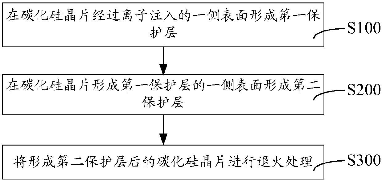
[0033] In one embodiment, such as figure 1 As shown, a silicon carbide activation annealing method is provided, comprising the following steps:

[0034] Step S100, forming a first protective layer on the surface of the silicon carbide wafer that has undergone ion implantation.

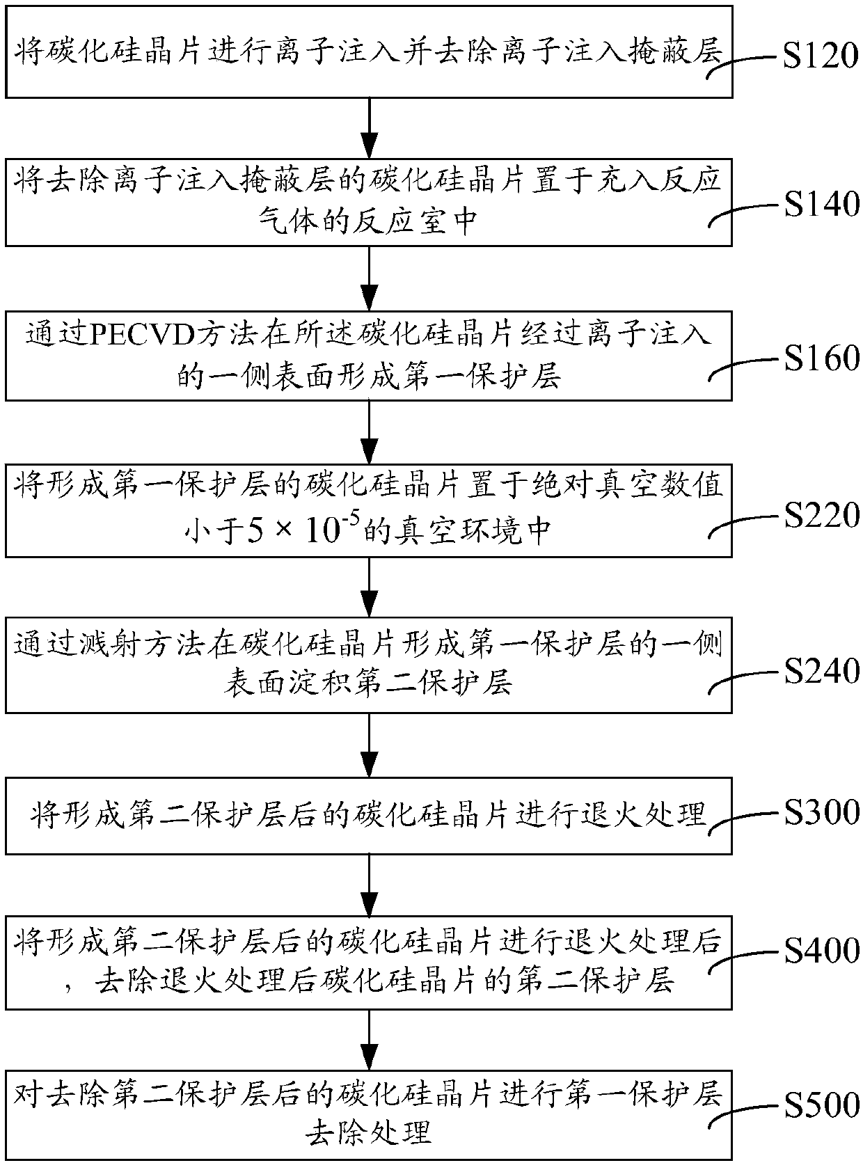
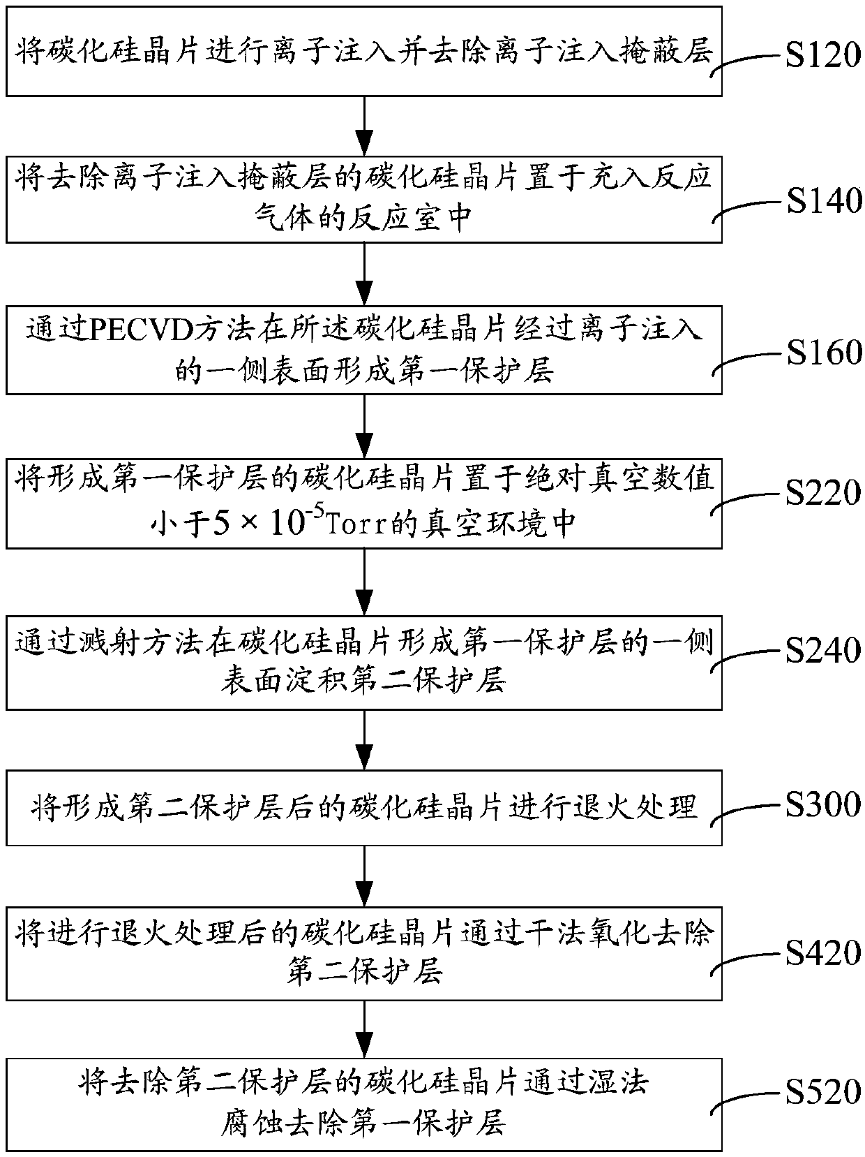
[0035] After the ion implantation is completed, the ion implantation masking layer is no longer useful and must be completely removed. The first protective layer is formed on the side surface where the ion implantation masking layer is removed, that is, the side surface where the silicon carbide wafer is manufactured to pr...


PUM

PropertyMeasurementUnit
thicknessaaaaaaaaaa
thicknessaaaaaaaaaa
thicknessaaaaaaaaaa

Abstract

The invention discloses a silicon carbide activation annealing method. The method comprises the following steps: forming a first protection layer on the surface, subjected to ion implantation, of oneside of a silicon carbide wafer; forming a second protective layer on the surface of one side, at which the first protective layer is formed, of the silicon carbide wafer; carrying out annealing treatment of the silicon carbide wafer with the second protection layer, wherein the thermal stability of the second protection layer is superior to that of the first protection layer during annealing treatment. A first protection layer and a second protection layer are formed on the surface of silicon carbide. During the annealing treatment of the silicon carbide wafer, the second protection layer canprevent the first protection layer from melting at a high temperature and prevents the sublimation of silicon atoms, and the first protection layer can effectively prevent silicon atoms on the surface of the silicon carbide wafer from sublimating and depositing again, so the problems of sublimation and deposition of silicon atoms on the surface of silicon carbide in the annealing process can be solved through the two protection layers, and the reliability of activating annealing protection of silicon carbide is improved.

Description

technical field [0001] The invention relates to the technical field of semiconductor device preparation, in particular to a silicon carbide activation annealing method. Background technique [0002] Due to its excellent physical properties and device characteristics, silicon carbide devices have made remarkable achievements in the development of power electronic devices. In the silicon carbide device manufacturing process, ion implantation technology is a key process to achieve doping. In order to eliminate the damage to the crystal lattice caused by implantation and activate the implanted impurities, it is necessary to anneal silicon carbide at a high temperature above 1500°C. At such a high temperature, the silicon carbide on the surface of the wafer will decompose, the silicon atoms will sublimate, and form Si, Si 2 C. SiC 2 Forms such as re-deposited on the surface of silicon carbide wafers, resulting in rough surface of the wafer, affecting the characteristics of sil...

Claims


Application Information

Patent Timeline
Patent Type & Authority Applications(China)
IPC IPC(8): H01L21/56H01L23/29H01L21/324
CPCH01L21/324H01L21/56H01L23/291H01L23/298
Inventor 张伟民甘新慧蒋正勇朱家从计建新
Owner WUXI CHINA RESOURCES MICROELECTRONICS
Why Eureka
Try Eureka