
Brightness enhancement film manufacturing method, backlight module, flat panel display and electronic device

A manufacturing method and technology of a brightness enhancement film, which are applied in the field of flat panel displays and electronic devices, and the field of brightness enhancement film manufacturing, can solve problems such as water ripples of the brightness enhancement film and affect the yield of backlight assembly, and achieve enhanced haze, reduction of water ripples and Interference fringe phenomenon, enhanced diffusion effect

Inactive Publication Date: 2019-07-09
惠州市聚飞光学材料有限公司
View PDF10 Cites 1 Cited by
  • Summary
  • Abstract
  • Description
  • Claims
  • Application Information

AI Technical Summary

Problems solved by technology

[0004] The main purpose of the present invention is to propose a method for manufacturing a brightness enhancement film, a backlight module, a flat panel display and an electronic device, aiming at solving the phenomenon of water ripples and interference fringes or doping in the brightness enhancement film in the prior art. Particles affect the yield of backlight assembly

Method used


Image

  • Brightness enhancement film manufacturing method, backlight module, flat panel display and electronic device
  • Brightness enhancement film manufacturing method, backlight module, flat panel display and electronic device
  • Brightness enhancement film manufacturing method, backlight module, flat panel display and electronic device

Examples


Embodiment Construction

[0027] It should be understood that the specific embodiments described here are only used to explain the present invention, not to limit the present invention.

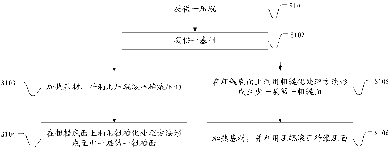
[0028] In order to solve the problem that in the prior art, the structure of the rough surface on the light-incoming side of the brightness enhancement film is relatively smooth, which cannot effectively increase the haze value, resulting in insufficient concealment, easy to produce water ripples, and the structure of the rough surface has certain rules. It is easy to produce problems such as interference fringes. This embodiment proposes a method for manufacturing a brightness enhancement film that can increase the haze value of the brightness enhancement film, enhance its concealing power, and reduce water ripples and interference fringes. figure 1 As shown, the brightness enhancing film manufacturing method includes:

[0029] S101, providing a pressing roller;

[0030] S102. Provide a substrate, the substrate incl...


PUM


Abstract

The invention discloses a brightness enhancement film manufacturing method, a backlight module, a flat panel display and an electronic device. With a method of, after a press roller and a substrate are provided, heating the substrate, using the press roller to roll the surface to be rolled and forming at least one first rough surface on the rough bottom by using a roughening treatment method, or amethod of, before the press roller rolls the surface to be rolled, forming at least one first rough surface on the rough bottom by using a roughening treatment method, the light-incident surface of the brightness enhancement film has a multi-layered rough surface structure, and the light emitted from the light source is necessary to pass through the multi-layered rough surface when passing through the brightness enhancement film manufactured by the brightness enhancement film manufacturing method provided by the invention, thereby enhancing the diffusion of the light incident. The brightnessenhancement film manufacturing method provided by the invention greatly enhances the haze of the light-incident surface of the brightness enhancement film and is beneficial to reduce the occurrence ofwater ripples and interference fringes. Moreover, since the substrate in the embodiment does not need to be doped with particles, the adverse effect on assembly yield is reduced.

Description

technical field [0001] The invention relates to the field of liquid crystal display, in particular to a method for manufacturing a brightness enhancement film, a backlight module, a flat panel display and an electronic device. Background technique [0002] At present, the brightness enhancement film is one of the most important optical films widely used in the backlight modules of liquid crystal displays. The functions of the brightness enhancement film include: improving light utilization, reducing light loss, increasing backlight brightness, and reducing power consumption The principle of the brightness enhancement film is mainly to use a special prism structure to concentrate the light. [0003] Although the brightness enhancement film produced according to the traditional method has the effect of improving the light utilization rate, it is prone to Moire effect and Newton ring phenomenon. In order to avoid these phenomena, an improved brightness enhancement film structur...

Claims


Application Information

Patent Timeline
Patent Type & Authority Applications(China)
IPC IPC(8): G02B5/04G02B5/02
CPCG02B5/0221G02B5/045
Inventor 邢其彬晏水平杨政宪
Owner 惠州市聚飞光学材料有限公司
Learn More