

Double-Resurf LDMOS With Drift And PSURF Implants Self-Aligned To A Stacked Gate "BUMP" Structure
a stacked gate and psurf technology, applied in the direction of transistors, electrical equipment, semiconductor devices, etc., can solve the problems of low breakdown voltage of ldmos transistors, high boron content, and high boron content, and achieve the highest possible bv to rdson ratio, facilitate ideal double-resurf performance, and improve the performance of ldmos transistors
- Summary
- Abstract
- Description
- Claims
- Application Information
AI Technical Summary
Benefits of technology
Problems solved by technology
Method used
Image

Examples
Embodiment Construction
[0030]The present invention relates to an improved LDMOS structure and fabrication method. The following description is presented to enable one of ordinary skill in the art to make and use the invention as provided in the context of a particular application and its requirements. As used herein, directional terms such as “above”, “below”, “upper”, “lower”, “vertical”, and “horizontal” are intended to provide relative positions for purposes of description, and are not intended to designate an absolute frame of reference. Various modifications to the preferred embodiment will be apparent to those with skill in the art, and the general principles defined herein may be applied to other embodiments. Therefore, the present invention is not intended to be limited to the particular embodiments shown and described, but is to be accorded the widest scope consistent with the principles and novel features herein disclosed.
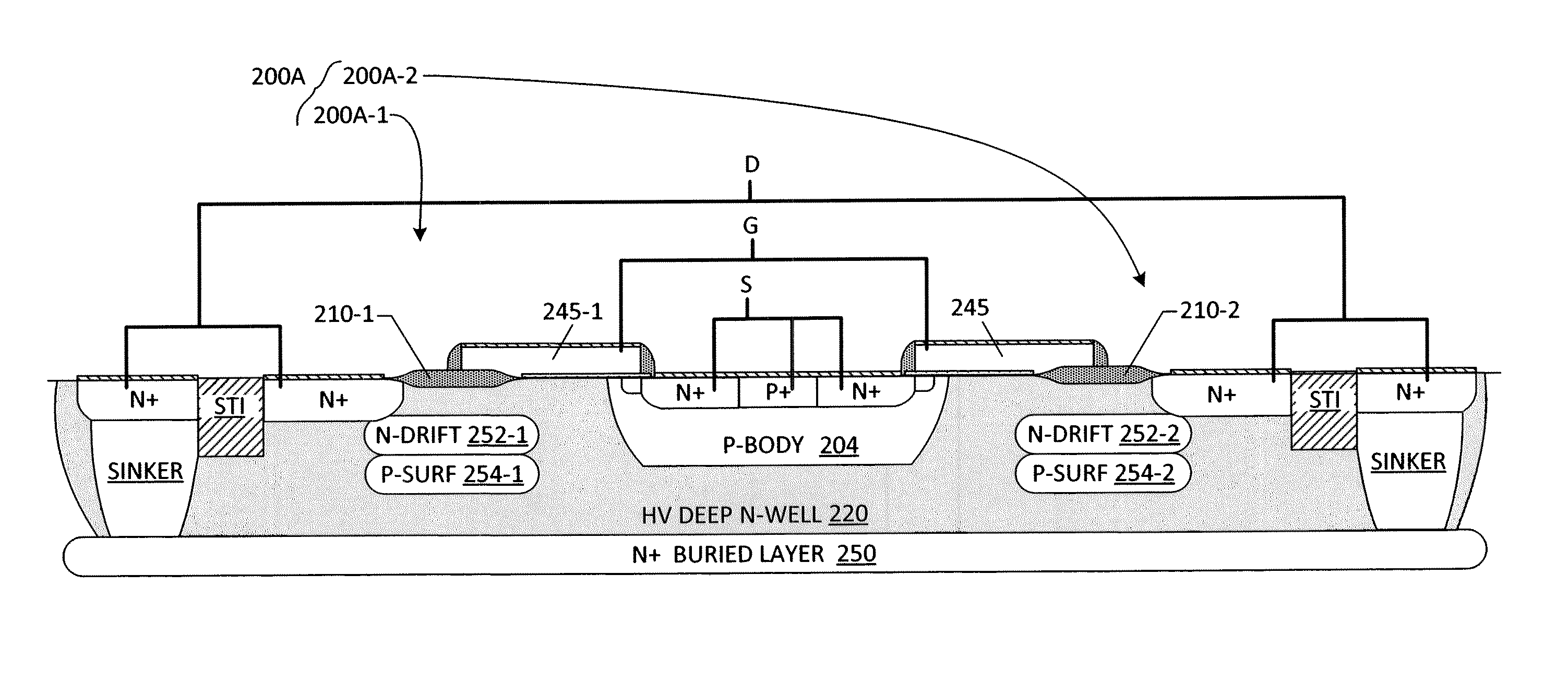
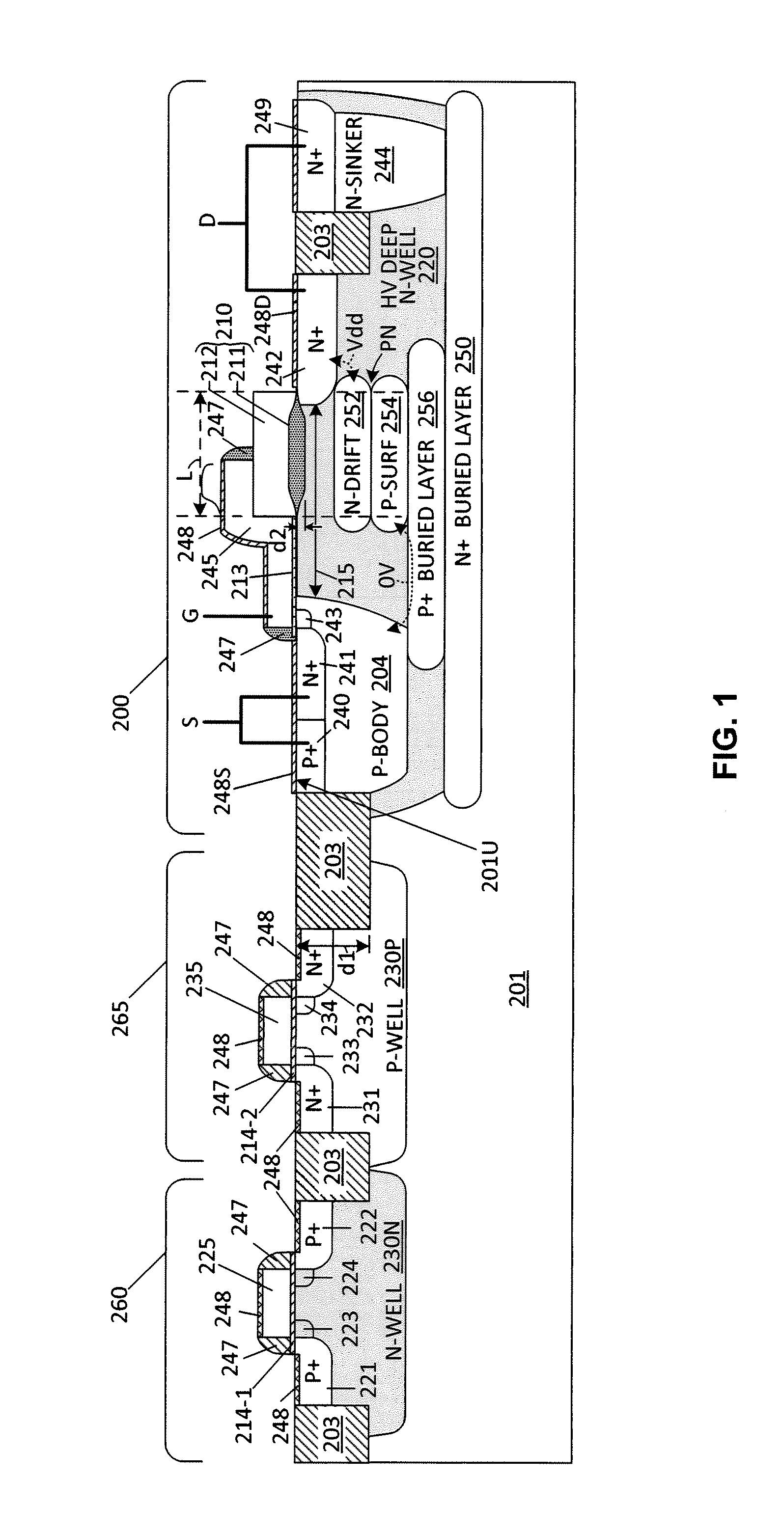
[0031]FIG. 1 is a cross-sectional view of a double-RESURF LDMOS transistor...
PUM
 Abstract
Description
Claims
Application Information