Display panel and display device for fingerprint identification
A display panel, fingerprint recognition technology, applied in character and pattern recognition, input/output process of data processing, instruments, etc., can solve the problem of large pixel circuit drive load, capacitive coupling, etc., to avoid parasitic capacitance and thickness increase , the effect of reducing the driving load
- Summary
- Abstract
- Description
- Claims
- Application Information
AI Technical Summary
Problems solved by technology
Method used
Image
Examples
Embodiment 1
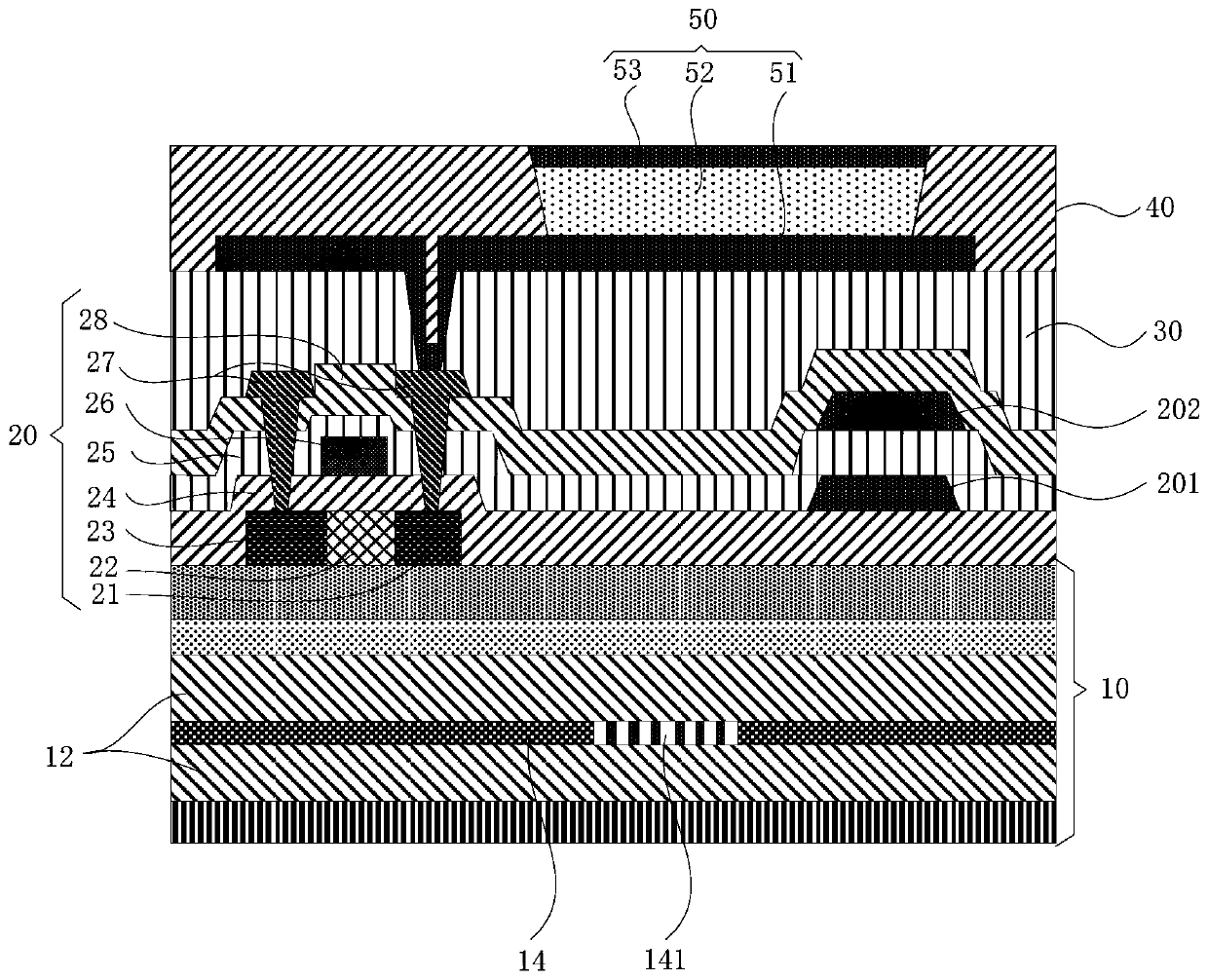
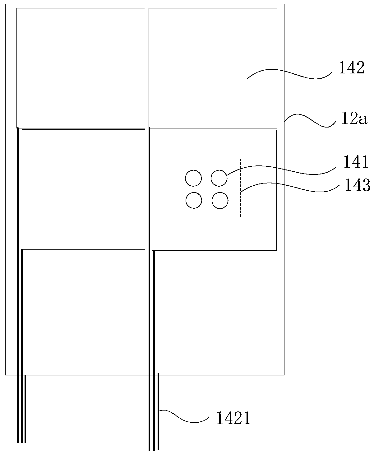
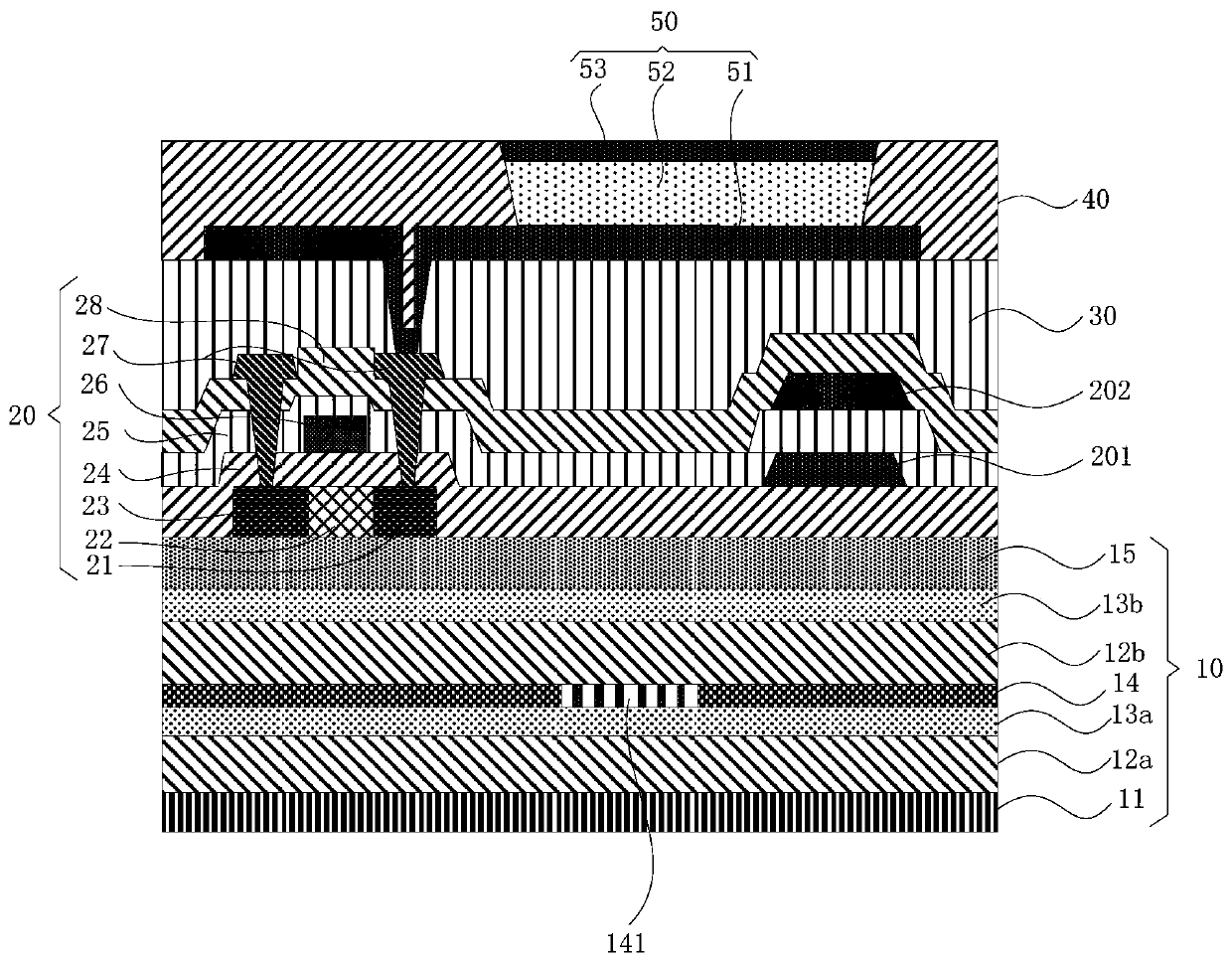
[0046] Figure 1A It is a schematic cross-sectional structure diagram of a display panel for fingerprint recognition provided by Embodiment 1 of the present invention, Figure 1B It is a schematic top view structural diagram of the conductive light-shielding layer in the display panel for fingerprint identification provided by Embodiment 1 of the present invention, Figure 1C Another schematic cross-sectional structure diagram of a display panel for fingerprint identification provided by Embodiment 1 of the present invention.
[0047] The inventor of the present invention found in the actual research process that there is a problem that the pixel circuit driving load is relatively large in the current fingerprint recognition display device, and the inventor found that the reason for this problem lies in: the existing fingerprint recognition display device , the metal light-shielding layer is often arranged on the PI layer in the array substrate or one of the metal layers in th...
Embodiment 2
[0068] Figure 2A It is a schematic cross-sectional structure diagram of a display panel for fingerprint identification provided by Embodiment 2 of the present invention, Figure 2B It is a schematic top view structure diagram of the conductive light-shielding layer in the display panel for fingerprint identification provided by Embodiment 2 of the present invention, Figure 2C Another schematic cross-sectional structure diagram of a display panel for fingerprint identification provided by Embodiment 2 of the present invention.
[0069] The display panel used for fingerprint identification provided by this embodiment is as follows: Figure 2A and Figure 2B As shown, the display panel includes an array substrate and several light emitting units 50 disposed on the array substrate, wherein the array substrate includes a substrate 10 and a thin film transistor (Thin Film Transistor, TFT for short) layer disposed on the substrate 10, wherein For the structure of the thin film t...
Embodiment 3
[0085] image 3 It is a schematic cross-sectional structure diagram of a display panel and a fingerprint recognition module in a display device provided by Embodiment 3 of the present invention.
[0086] Embodiment 3 of the present invention provides a display device. The display device can be an OLED display device and any product with a display function such as a TV, a digital camera, a mobile phone, a tablet computer, a smart watch, an e-book, a navigator, or the like that includes an OLED display device. part.
[0087] Wherein, in this embodiment, the display device includes a fingerprint identification module 60 and the display panel described in any of the above-mentioned embodiments. In this embodiment, the structure, function and realization of the display panel can refer to the specific description in the above-mentioned embodiments. No more details here, wherein, the fingerprint recognition module 60 is located below the display panel and corresponds to the imaging ...
PUM
 Abstract
Description
Claims
Application Information


