Packaging structure, preparation method of packaging structure and organic light-emitting display
A packaging structure and organic technology, applied in circuits, electrical components, electrical solid devices, etc., can solve the problems of large thickness and non-compliance with requirements, and achieve the effect of simplifying the process, avoiding the intrusion of water and oxygen, and improving the impact resistance.
- Summary
- Abstract
- Description
- Claims
- Application Information
AI Technical Summary
Problems solved by technology
Method used
Image
Examples
Embodiment 1
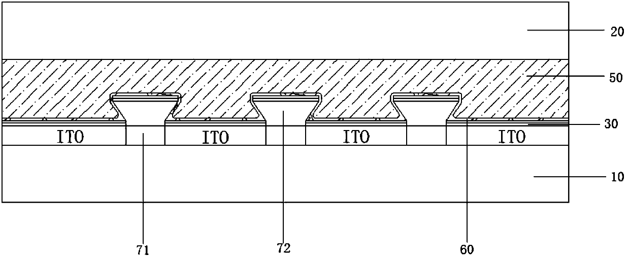
[0040] An embodiment of the present invention provides a packaging structure, such as figure 2 As shown, it includes a first substrate 10 and a second substrate 20 arranged oppositely; a body to be packaged 30 arranged between the first substrate 10 and the second substrate 20; The encapsulation layer 60 covering the exposed surface of the to-be-packaged body 30; wherein the to-be-packaged body 30 is formed on the first substrate 10, and the outer side of the to-be-packaged body 30 relative to the first substrate 10 forms the In addition, on the first substrate 10 or the encapsulation layer 60, an encapsulation ring 40 is also arranged around the outer peripheral edge of the object to be encapsulated 30, and the encapsulation ring 40 is arranged on the first substrate 10 (or the encapsulation layer 60) A closed cavity is enclosed between the second substrate 20 and the second substrate 20 . Wherein, a desiccant layer 50 is interposed between the encapsulation layer 60 and th...
Embodiment 2
[0053] The embodiment of the present invention provides an organic electroluminescent device, which is different from the embodiment 1 in that the package body 30 is an organic light emitting array layer.
[0054] Such as image 3 As shown, the organic light-emitting array layer includes: a first electrode layer and spacer columns 72, and the first electrode layer includes a plurality of first electrode strips arranged parallel to each other (the first electrode layer is an anode layer in the figure, for example ITO layer), the extension direction of the isolation column 72 is perpendicular to the extension direction of the first display electrode; wherein the isolation column 72 has an inverted trapezoidal cross-section along the extension direction of the first electrode strip, The acute angle between each side in the cross section and the first electrode layer is 45°-70°. In the present invention, setting the spacer column 72 in such a structure is conducive to a good sepa...
Embodiment 3
[0066] An embodiment of the present invention provides a method for preparing an organic electroluminescent device, comprising the following steps:
[0067] Step S11, preparing an organic light-emitting array layer on the first substrate. For the structure of the organic light-emitting array layer, refer to the previous description;
[0068] Step S12 , forming a continuous encapsulation layer covering the exposed surface of the organic light emitting array layer (the surface away from the first substrate) on the first substrate.
[0069] Form an encapsulation layer 60 that continuously covers the organic light-emitting array layer and is away from the surface of the first substrate. The encapsulation layer 60 extends to the surface of the first substrate 10 to form a closed cavity with the first substrate 10. The organic light-emitting array layer is encapsulated in the inside a closed cavity.
[0070] Step S13 , disposing an encapsulation ring on the encapsulation layer arou...
PUM
 Abstract
Description
Claims
Application Information


