


Quick Research
Generate reliable direction feasibility study reports for your R&D in just a few steps.

Technical Q&A
Discover and master advanced knowledge NOW. Basics, ideas, possibilities, all at once.

Find Solutions
As an expert in R&D theories, this can generate solutions to your technical problems instantly.

Evaluate Feasibility
Analyze your overall solution with one click, know your potential R&D risks in advance.

Monitor Landscape
Get weekly tech updates, stay abreast of the latest tech innovations and key insights.
Printed circuit board for a radar level measurement device with waveguide coupling
A technology of level measurement and circuit board, which is applied in the direction of measuring devices, radio wave measurement systems, waveguides, etc., to achieve the effect of preventing environmental influence and benefiting mechanical stability
- Summary
- Abstract
- Description
- Claims
- Application Information
AI Technical Summary
Problems solved by technology
Method used
Image

Examples
Embodiment Construction
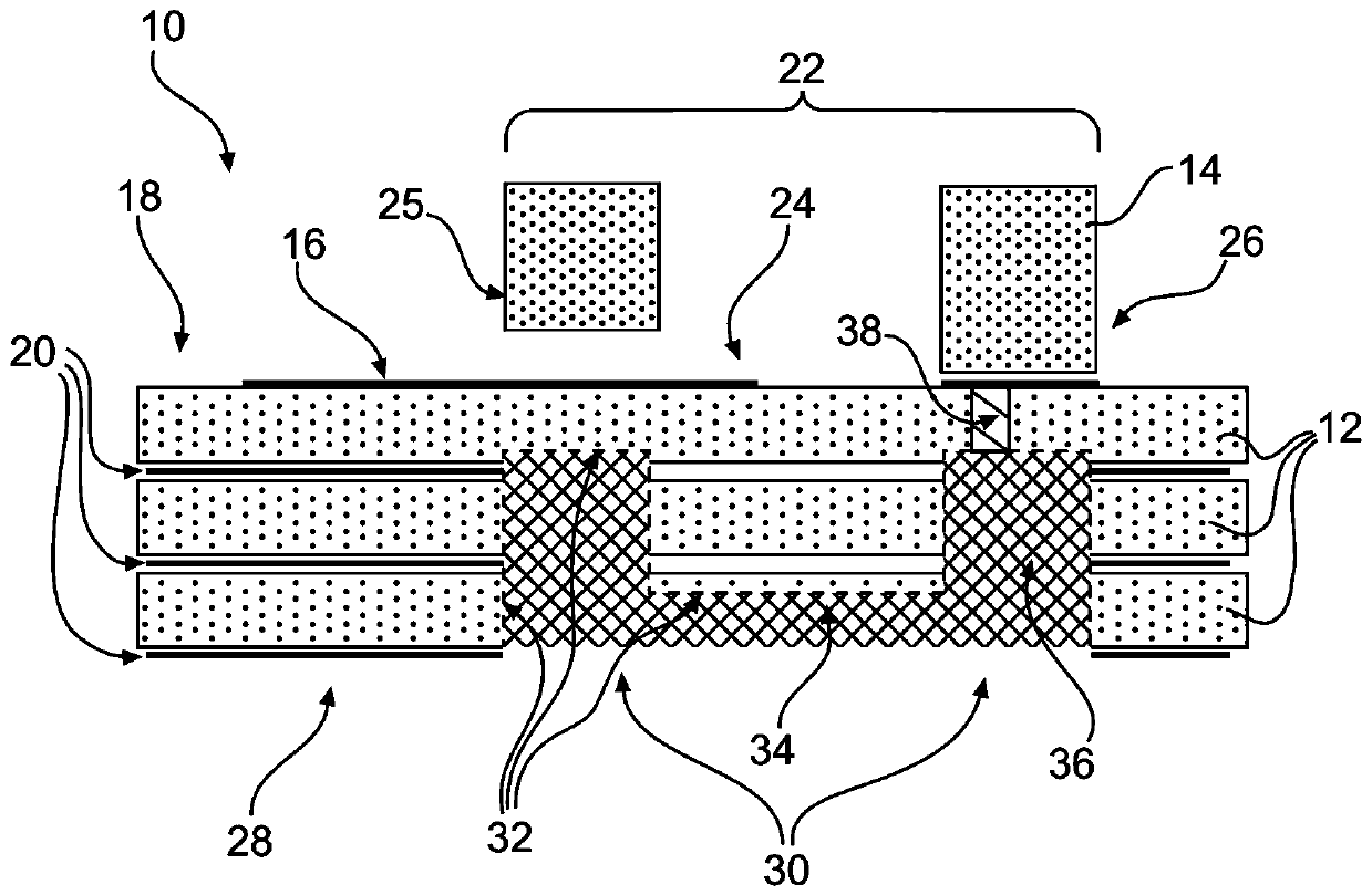
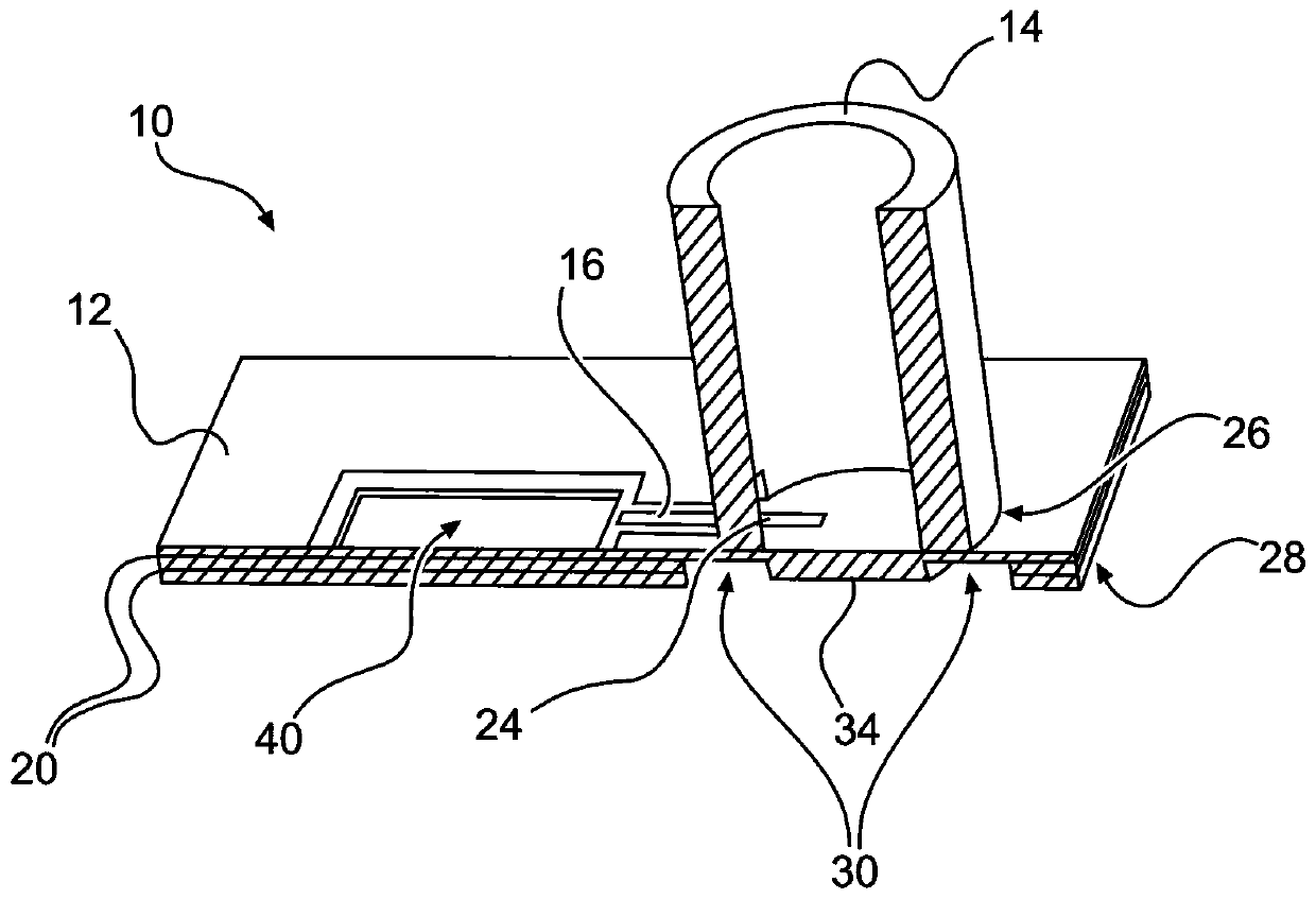
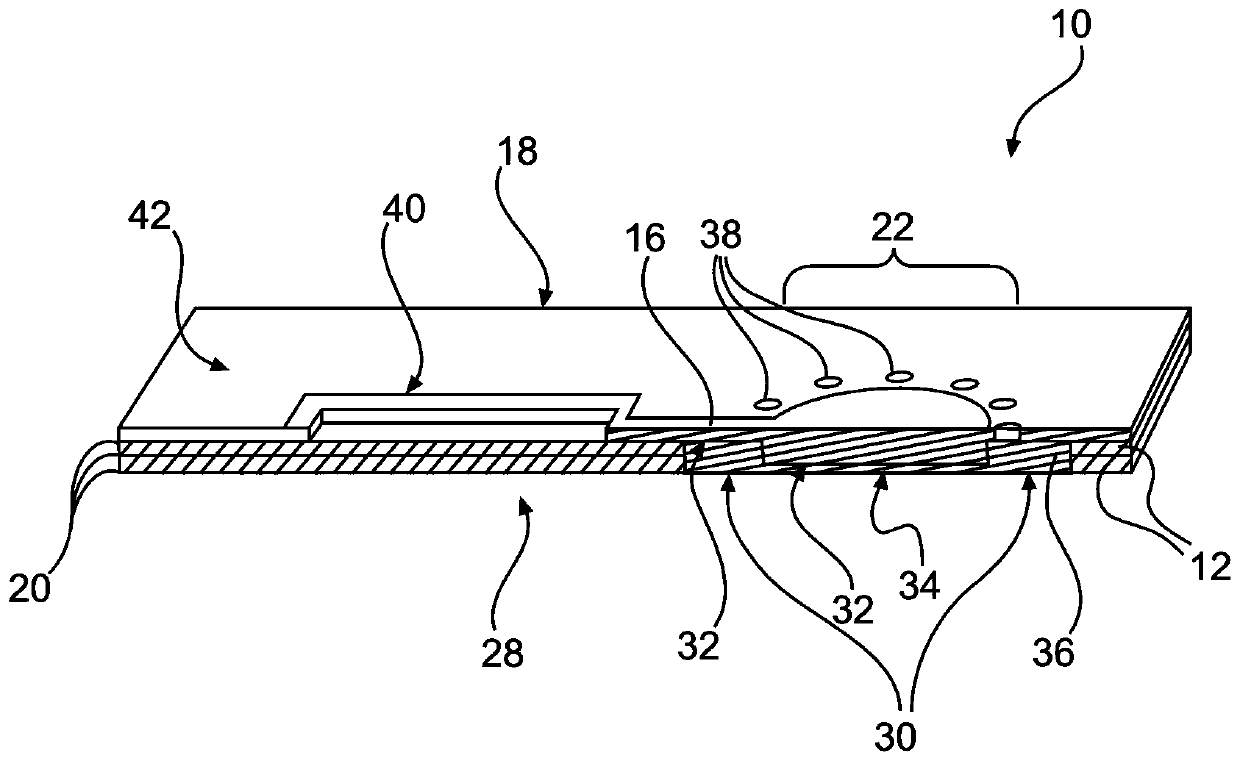
[0040] figure 1 A partial area of the circuit board 10 for coupling waveguides 14 is shown. A microwave conductor 16 is arranged on the circuit board substrate 12 . In the example shown here, the microwave conductor 16 extends over the surface of the circuit board substrate 12 , here the microwave conductor 16 extends over the front side 18 . According to one example (not shown here), the microwave conductor 16 is arranged inside the circuit board substrate 12 . The advantage is that, with figure 1 Contrary to what is shown, there is no need to separate or shorten the waveguide 14 at this location additionally for the purpose of insulation, but the waveguide 14 has a circumferential planar or flat end face, the advantage of which is simple manufacturing (for example, cutting ).
[0041] The circuit board substrate 12 is made of a material that is inactive for high frequencies or is insulating for the relevant high frequency range (for example LCP or PTFE substrates of va...
PUM
 Abstract
Description
Claims
Application Information
 - R&D Engineer
- R&D Manager
- IP Professional
- Industry Leading Data Capabilities
- Powerful AI technology
- Patent DNA Extraction
Browse by: Latest US Patents, China's latest patents, Technical Efficacy Thesaurus, Application Domain, Technology Topic, Popular Technical Reports.
© 2024 PatSnap. All rights reserved.Legal|Privacy policy|Modern Slavery Act Transparency Statement|Sitemap|About US| Contact US: help@patsnap.com