
Convolution operation based on analog matrix operation unit and application thereof

A matrix operation and convolution operation technology, applied in the field of convolution operation, can solve the problems of consuming operation time and power consumption, computing unit and memory resource consumption, etc., to achieve area reduction, high computing parallelism, practicability and applicability strong effect

Active Publication Date: 2019-07-12
HEFEI HENGSHUO SEMICON CO LTD
View PDF11 Cites 18 Cited by
  • Summary
  • Abstract
  • Description
  • Claims
  • Application Information

AI Technical Summary

Problems solved by technology

There are two major problems with this architecture: during the calculation process, the round-trip transmission of on-chip and off-chip data consumes a lot of computing time and power consumption, and the data transfer between the computing unit and the memory consumes a lot of resources; in order to meet the needs of computing power There is a contradiction between the ever-increasing number of parallel computing units and the bandwidth of storage units, which has become a bottleneck for the improvement of the computing power of AI chips

Method used


Image

  • Convolution operation based on analog matrix operation unit and application thereof
  • Convolution operation based on analog matrix operation unit and application thereof
  • Convolution operation based on analog matrix operation unit and application thereof

Examples


Embodiment 1

[0091] like figure 1 As shown, it is a single analog multiplication circuit that constitutes an analog matrix operation unit in this embodiment, including a pair of floating gate field effect transistors M 1 , M 2 and a differential current sense circuit;

[0092] where M 1 and M 2The common gate is connected to the voltage source, and the common drain or common source is connected to the analog voltage input. The differential current detection circuit includes two current input terminals and one output terminal, and the two current input terminals are correspondingly connected to M 1 and M 2 respective source or drain; it is stated here that if M 1 and M 2 The common drain is connected to the analog voltage input, and the two current input terminals are correspondingly connected to M 1 and M 2 respective sources, if M 1 and M 2 The common source is connected to the analog voltage input, and the two current input terminals are correspondingly connected to M 1 and M ...

Embodiment 2

[0131] refer to Figure 12 , is a schematic diagram of a 2D convolution operation based on an analog matrix operation unit in this embodiment: the dimension of the input feature map is 5×5, the dimension of the output feature map is 3×3, and the dimension of the convolution kernel is 3×3 , without considering the bias bias.

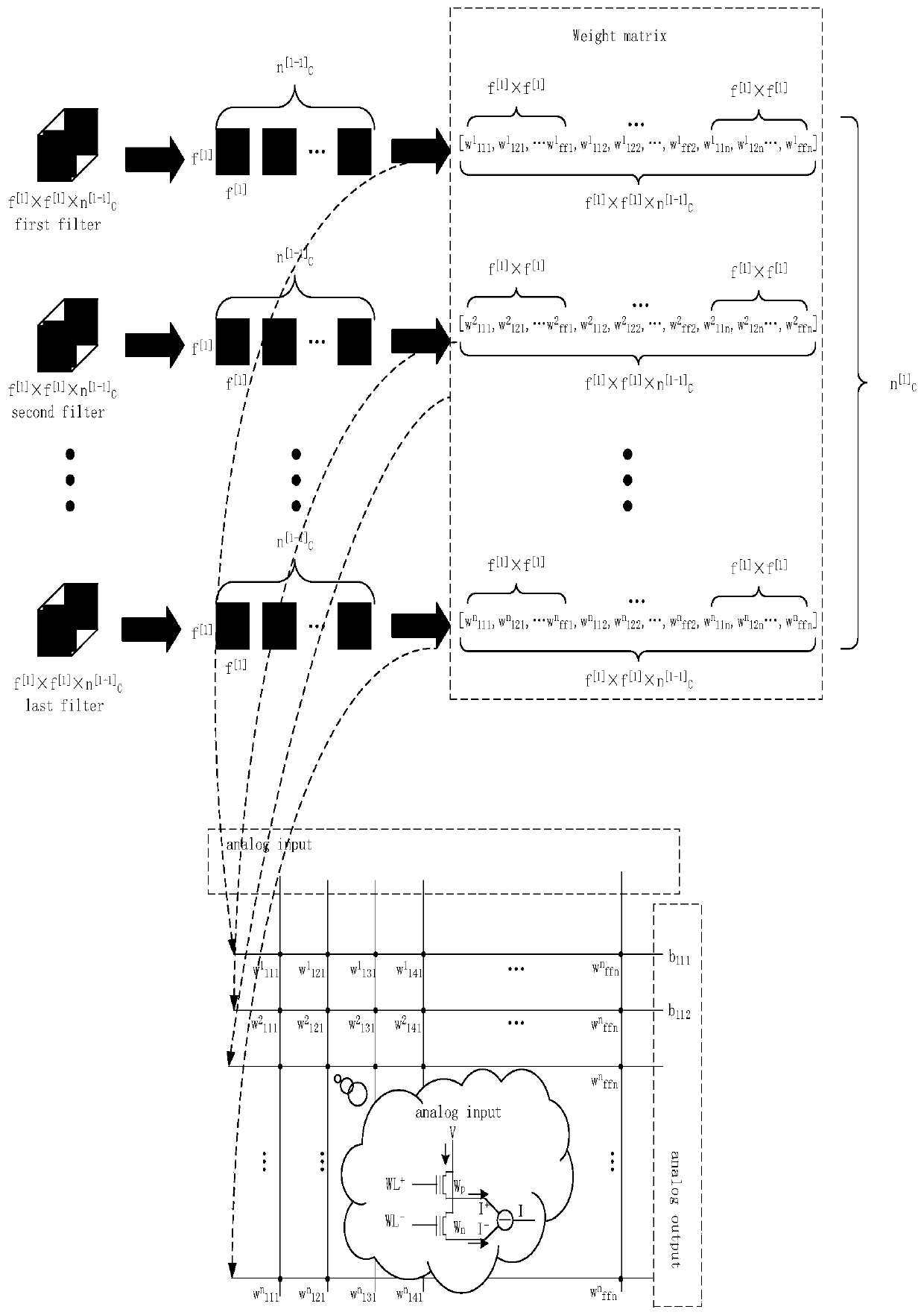
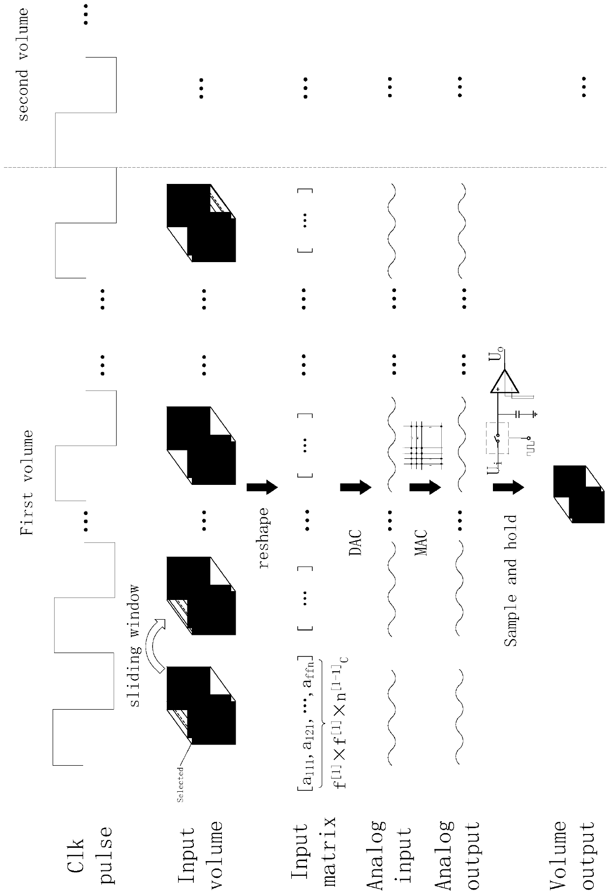
[0132] Figure 13 It is the schematic diagram of the 2D convolution realized by the analog matrix operation unit; the convolution kernel with a size of 3×3 is converted into a horizontal quantity [w 11 ,w 12 ,w 13 ,w 21 ,w 22 ,w 23 ,w 31 ,w 32 ,w 33 ] to map it to a row of the analog matrix operation unit; convert the input feature map into 9 horizontal quantities according to the sliding window, namely [a 11 ,a 12 ,a 13 ,a 21 ,a 22 ,a 23 ,a 31 ,a 32 ,a 33 ], [a 12 ,a 13 ,a 14 ,a 22 ,a 23 ,a 24 ,a 32 ,a 33 ,a 34 ], ..., [a 33 ,a 34 ,a 35 ,a 43 ,a 44 ,a 45 ,a 53 ,a 54 ,a 55 ], convert it into an analog voltage, and then ...

Embodiment 3

[0134] refer to Figure 14 , which is a schematic diagram of implementing a specific 3D convolution operation based on the analog matrix operation unit in this embodiment:

[0135] The dimension of the input feature map is 3×3×3, and the dimension of the output feature map is 3×3×2. Two 1×1×3 convolution kernels and two 1×1×1 biases are used.

[0136] refer to Figure 15 , is the schematic diagram of the 3D convolution realized by the analog matrix operation unit, which converts two convolution kernels with a size of 1×1×3 and two biases of 1×1×3 into two horizontal quantities [w 11 ,w 12 ,w 13 ,b 1 ], [w 21 ,w 22 ,w 23 ,b 2 ], map it to the two lines of the analog matrix operation unit; convert the input feature map into 9 horizontal quantities according to the sliding window, namely [a 111 ,a 112 ,a 113 ,1], [a 121 ,a 122 ,a 123 ,1],...,[a 331 ,a 332 ,a 333 ,1]. It is converted into an analog voltage, and then input in parallel sequence from the analog inpu...


PUM


Abstract

The invention relates to the technical field of circuit design, and discloses a convolution operation based on an analog matrix operation unit and application thereof. the convolution operation is used for converting and splicing convolution kernels into P transverse quantities with the length of Q and mapping the transverse quantities into an analog matrix operation unit, inputting a characteristic pattern, segmenting the characteristic pattern according to a sliding window, converting the characteristic pattern into N transverse variables with the length of Q, sequentially mapping the N transverse variables with the length of Q into vectors under a pulse wave, and simultaneously outputting N operation results with the length of P through a sampling retainer to obtain a complete convolution result and outputting the convolution result. According to the method, the convolution calculation rate is effectively increased, the power consumption and the circuit area are reduced, high calculation parallelism is achieved, the calculation density and efficiency are greatly improved, and the method has high practical value and wide application prospects.

Description

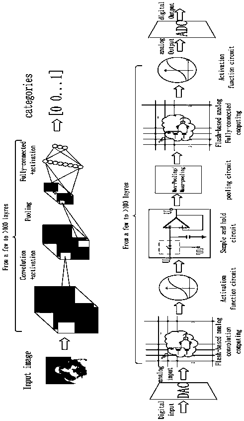
technical field [0001] The invention relates to the technical field of circuit design, in particular to a convolution operation based on an analog matrix operation unit and its application. Background technique [0002] Convolutional neural networks have shown great advantages in image recognition, object detection, and many machine learning applications. The convolutional neural network is mainly composed of a convolutional layer, a pooling layer, and a cascade of fully connected layers. It mainly includes the convolution operation between the input layer pixel block and the convolution kernel, the activation operation for introducing nonlinearity, and the reduction of features. The downsampling operation (that is, pooling) on ​​the feature map and the full connection operation after convolution, among which most of the calculations are in the convolutional layer and the full connection layer. [0003] Large convolutional neural networks with huge parameter sets and comput...

Claims


Application Information

Patent Timeline
IPC IPC(8): G06F17/16G06N3/063
CPCG06F17/16G06N3/063
Inventor 任军徐伟民蒋明峰李政达吕向东徐培
Owner HEFEI HENGSHUO SEMICON CO LTD
Learn More