Supercharge Your Innovation With Domain-Expert AI Agents!

Thin film transistor (TFT), manufacturing method thereof, array substrate, display panel and display device

A technology of thin film transistor and manufacturing method, which is applied in transistor, semiconductor/solid-state device manufacturing, semiconductor device and other directions, can solve the problems of increased contact resistance, RC delay, large power consumption, etc., and achieves the effect of enhancing connection performance

Active Publication Date: 2019-07-12
CHENGDU BOE OPTOELECTRONICS TECH CO LTD +1
View PDF7 Cites 2 Cited by
  • Summary
  • Abstract
  • Description
  • Claims
  • Application Information

AI Technical Summary

Problems solved by technology

[0004] The invention provides a thin film transistor, a manufacturing method, an array substrate, a display panel, and a display device to improve the display panel of the prior art. When the resolution is continuously improved, the contact resistance between the active layer and the source-drain layer wiring Further increase, and eventually serious RC delay, large power consumption problems

Method used


Image

  • Thin film transistor (TFT), manufacturing method thereof, array substrate, display panel and display device
  • Thin film transistor (TFT), manufacturing method thereof, array substrate, display panel and display device
  • Thin film transistor (TFT), manufacturing method thereof, array substrate, display panel and display device

Examples


Embodiment Construction

[0039] The implementation process of the embodiment of the present invention will be described in detail below in conjunction with the accompanying drawings. It should be noted that the same or similar reference numerals represent the same or similar elements or elements having the same or similar functions throughout. The embodiments described below by referring to the figures are exemplary only for explaining the present invention and should not be construed as limiting the present invention.

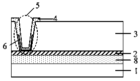
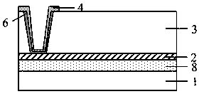
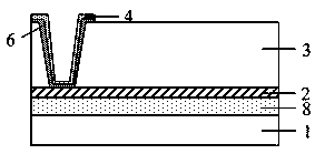
[0040] see figure 1 , an embodiment of the present invention provides a thin film transistor, comprising: an active layer 2, an insulating layer 3, and a source-drain layer 4 sequentially stacked on a base substrate 1, wherein the source-drain layer 4 passes through the insulating layer The through hole 5 of 3 conducts with the active layer 2;

[0041] There is a transition layer 6 at the position of the through hole 5 between the source and drain layer 4 and the active layer 2, the...


PUM


Abstract

The invention discloses a TFT, a manufacturing method thereof, an array substrate, a display panel and a display device, and aims at the problems including increase of the contact resistance of wiresbetween active layer and source / drain electrode layer with increase of the resolution and further severe RC delay and large power consumption in a display panel in the prior art. The TFT comprises anactive layer, an insulating layer and a source / drain electrode layer arranged on a substrate successively, the source / drain electrode layer is connected to the active layer by penetrating a through hole in the insulating layer, a transition layer is arranged between the source / drain electrode layer and active layer in the through hole position, the transition layer covers the bottom of the throughholes and at least part of sidewall of the through hole, and the transition layer of an integrated structure comprises elements of the active layer and elements of a first film layer.

Description

technical field [0001] The present invention relates to the technical field of semiconductors, in particular to a thin film transistor and a manufacturing method, an array substrate, a display panel, and a display device. Background technique [0002] Flat panel display (F1at Pane1 Display, FPD) has become the mainstream product in the market, and there are more and more types of flat panel displays, such as liquid crystal display (Liquid Crystal Display, LCD), organic light emitting diode (Organic Light Emitted Diode, OLED) display , Plasma Display Panel (P1asma DisplayPane1, PDP) and Field Emission Display (Field Emission Display, FED), etc. [0003] With the continuous improvement of resolution, the signal trace width and via hole size of the display panel will continue to decrease, which will lead to a further increase in the contact resistance between the active layer and the source-drain layer traces, and eventually serious RC Latency, power consumption big problem. ...

Claims


Application Information

Patent Timeline
Patent Type & Authority Applications(China)
IPC IPC(8): H01L29/786H01L29/417H01L21/336
CPCH01L29/78618H01L29/41733H01L29/66757H01L29/458H10K59/1213H01L21/28518H01L27/1222H01L29/78675H10K77/111H10K2102/311
Inventor 包征陈功辛燕霞胡红伟吴奕昊张祎杨赵广洲
Owner CHENGDU BOE OPTOELECTRONICS TECH CO LTD
Features
  • R&D
  • Intellectual Property
  • Life Sciences
  • Materials
  • Tech Scout
  • Unparalleled Data Quality
  • Higher Quality Content
  • 60% Fewer Hallucinations
Learn More