Semiconductor structure and forming method thereof

A semiconductor and device structure technology, applied in the direction of semiconductor devices, semiconductor/solid-state device components, electric solid-state devices, etc., can solve the problems of complex formation methods of semiconductor structures, and achieve the effect of simplifying the formation methods

Active Publication Date: 2019-07-19
SEMICON MFG INT (SHANGHAI) CORP +1
View PDF6 Cites 5 Cited by
  • Summary
  • Abstract
  • Description
  • Claims
  • Application Information

AI Technical Summary

Problems solved by technology

[0004] However, the formation method of the semiconductor structure in the prior art is complicated

Method used


Image

  • Semiconductor structure and forming method thereof
  • Semiconductor structure and forming method thereof
  • Semiconductor structure and forming method thereof

Examples


Embodiment Construction

[0031] As mentioned in the background, the overlay accuracy of the semiconductor structure formed in the prior art is relatively low.

[0032] Figure 1 to Figure 3 It is a structural schematic diagram of each step of a method for forming a semiconductor structure.

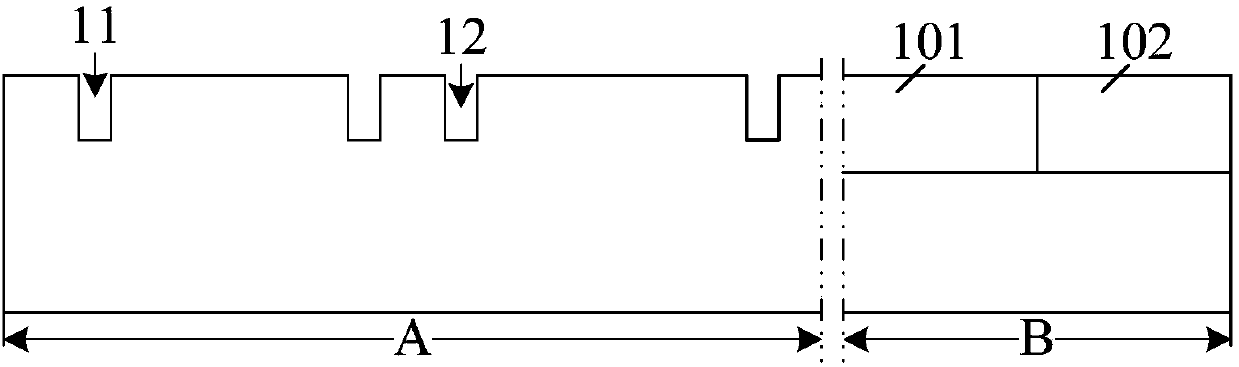
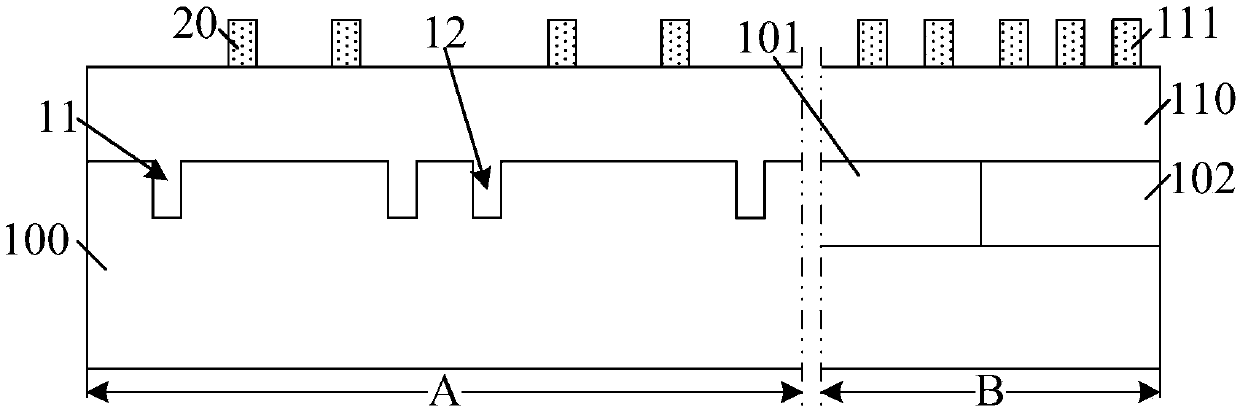
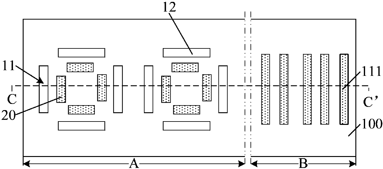
[0033] Please refer to figure 1 , providing a substrate 100, the substrate 100 includes a device region B and a marking region A; a first active region 101 is formed in the device region B substrate 100, and a first active region 101 is formed in the marking region A substrate A mark 11 ; forming a second active region 102 in the device region B substrate 100 , and forming a second mark 12 in the mark region A substrate 100 .

[0034] Please refer to figure 2 and image 3 , image 3 yes figure 2 Forming a gate layer 110 on the substrate 100 in the device region B and the marking region A along the cutting line CC'; forming a photoresist layer on the gate layer 110 in the device region B and the marking regio...


PUM

PropertyMeasurementUnit
widthaaaaaaaaaa

Abstract

The invention discloses a semiconductor structure and a forming method thereof. The method comprises the following steps: forming a first device structure and a second device structure in a device region, and forming a mark structure in the mark region, wherein the mark region has a first rotating center, the mark region comprises a plurality of mark parts, each marking part comprises a first branch part and a second branch part, and the first branch parts are used for marking a first device, and the second branch parts are used for marking a second device structure; and forming a first graphical layer on the device region, and forming a test mark on the mark region. The forming method can improve the performance of the formed semiconductor structure.

Description

technical field [0001] The invention relates to the technical field of semiconductor manufacturing, in particular to a semiconductor structure and a forming method thereof. Background technique [0002] In the existing semiconductor manufacturing process, it is usually necessary to form patterns on multi-layer film layers to form semiconductor devices with certain functions. There is a certain alignment relationship between the patterns of different film layers, and a method of forming an alignment mark on the wafer is usually adopted, and the alignment is realized through the alignment mark. [0003] In the prior art, due to the influence of factors such as the wafer offset vector or focusing accuracy in the photolithography process, the photoresist will be exposed during the exposure process, resulting in offset vectors, rotation, scaling, or normalization of the pattern after exposure. issues such as delivery. Therefore, in the process of forming a semiconductor structu...

Claims


Application Information

Patent Timeline
Patent Type & Authority Applications(China)
IPC IPC(8): H01L23/544G03F9/00
CPCG03F9/7046H01L23/544H01L2223/54426
Inventor 舒强
Owner SEMICON MFG INT (SHANGHAI) CORP
Why Eureka
Try Eureka