Dielectric layer of ultra-low dielectric constant and forming method thereof
A technology with ultra-low dielectric constant and low dielectric constant, which is applied in the direction of circuits, electrical components, electric solid devices, etc., and can solve the problem of poor adhesion, poor step coverage of metal dielectric barrier layers, and influence on metallization process Electrical performance and reliability and other issues, to achieve the effect of good electrical performance and reliability, low tensile stress
- Summary
- Abstract
- Description
- Claims
- Application Information
AI Technical Summary
Problems solved by technology
Method used
Image

Examples
no. 1 example
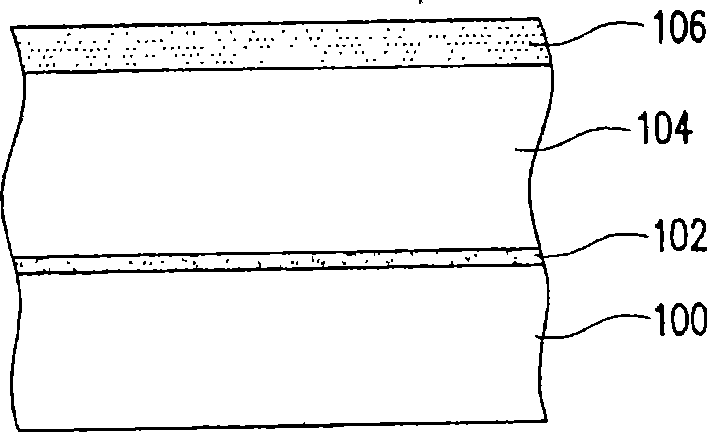
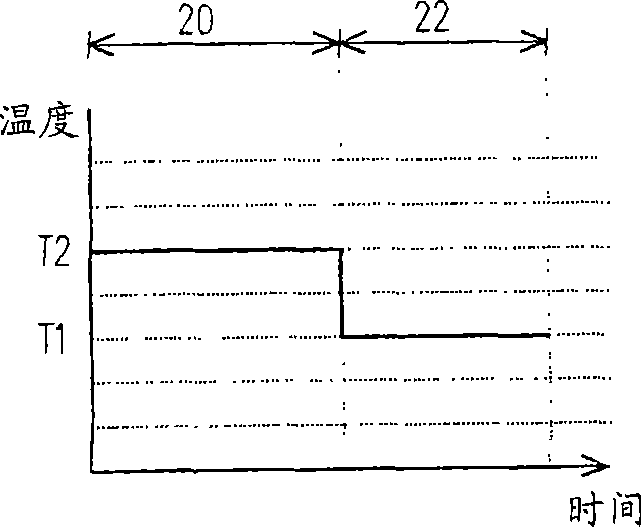
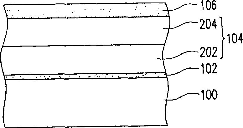
[0065] In this embodiment, the temperature change program is a gradient temperature change program including two temperature stages, such as figure 2 shown. exist figure 2 Among them, the two temperature stages include a first temperature stage 20 and a second temperature stage 22 in sequence, wherein the first temperature stage 20 is a high temperature stage; the second temperature stage 22 is a low temperature stage. The temperature of each stage 20, 22 is related to the dielectric matrix (DielectricMatrix) used. In one embodiment, the temperature of the first temperature stage 20 is, for example, between 250 and 350 degrees Celsius; the temperature of the second temperature stage 22 is, for example, between 200 and 250 degrees Celsius. In one embodiment, the same main chain precursor and the same porogen are introduced during the deposition process of the first temperature stage 20 and the second temperature stage 22 .
[0066] Each stage 20, 22 can be performed on-sit...
no. 2 example
[0073] In this embodiment, the temperature change program is a gradient temperature change program including two temperature stages, such as image 3 shown. exist image 3 Among them, the two temperature stages include a first temperature stage 30 and a second temperature stage 32 in sequence, wherein the first temperature stage 30 is a low temperature stage; the second temperature stage 32 is a high temperature stage. The temperature at each stage 30, 32 is related to the dielectric substrate used. In one embodiment, the temperature of the low temperature stage is about 200 to 250 degrees Celsius; the temperature of the high temperature stage is about 250 to 350 degrees Celsius. In one embodiment, when performing the deposition process in the first temperature stage 30 and the second temperature stage 32, the same main chain precursor and the same porogen are introduced.
[0074]Each stage 30, 32 can be performed on-site in the same deposition tool or off-site in a differe...
no. 3 example
[0080] In this embodiment, the temperature change program is a gradient temperature change program including three temperature stages, such as Figure 4 shown. exist Figure 4 Among them, these three temperature stages include the first temperature stage 40, the second temperature stage 42 and the third temperature stage 44 carried out in sequence, wherein, the first temperature stage 40 is a low temperature stage; the second temperature stage 42 is a high temperature stage stage; the third temperature stage 44 is also a low temperature stage. The temperature of the second temperature stage 42 is higher than the temperature of the first temperature stage 40 and the third temperature stage 44 . The temperatures of the first temperature stage 40 and the third temperature stage 44 can be the same or different, and only the first temperature stage 40 and the third temperature stage 44 having the same temperature are shown in the figure. The temperature at each stage is related ...
PUM
| Property | Measurement | Unit |
|---|---|---|
| Tensile stress | aaaaa | aaaaa |
Abstract
Description
Claims
Application Information