Three-dimensional memory preparation method, three-dimensional memory and electronic device

A memory, three-dimensional technology, applied in circuits, electrical components, electric solid-state devices, etc., can solve the problems of increasing the production time of three-dimensional memory, prolonging the production cycle, increasing production costs, etc., achieving a simple structure, improving profits, and reducing time and costs. Effect

Inactive Publication Date: 2019-07-23
YANGTZE MEMORY TECH CO LTD
View PDF3 Cites 13 Cited by
  • Summary
  • Abstract
  • Description
  • Claims
  • Application Information

AI Technical Summary

Problems solved by technology

With the continuous development of three-dimensional memory, the composition and structure of three-dimensional memory are becoming more and more complex, so the process steps will inevitably be increased during the preparation, the production cost will be increased, and the productio

Method used


Image

  • Three-dimensional memory preparation method, three-dimensional memory and electronic device
  • Three-dimensional memory preparation method, three-dimensional memory and electronic device
  • Three-dimensional memory preparation method, three-dimensional memory and electronic device

Examples


Embodiment Construction

[0039] The following are the preferred embodiments of the present invention. It should be pointed out that for those of ordinary skill in the art, without departing from the principle of the present invention, several improvements and modifications can be made, and these improvements and modifications are also regarded as the present invention. The scope of protection of the invention.

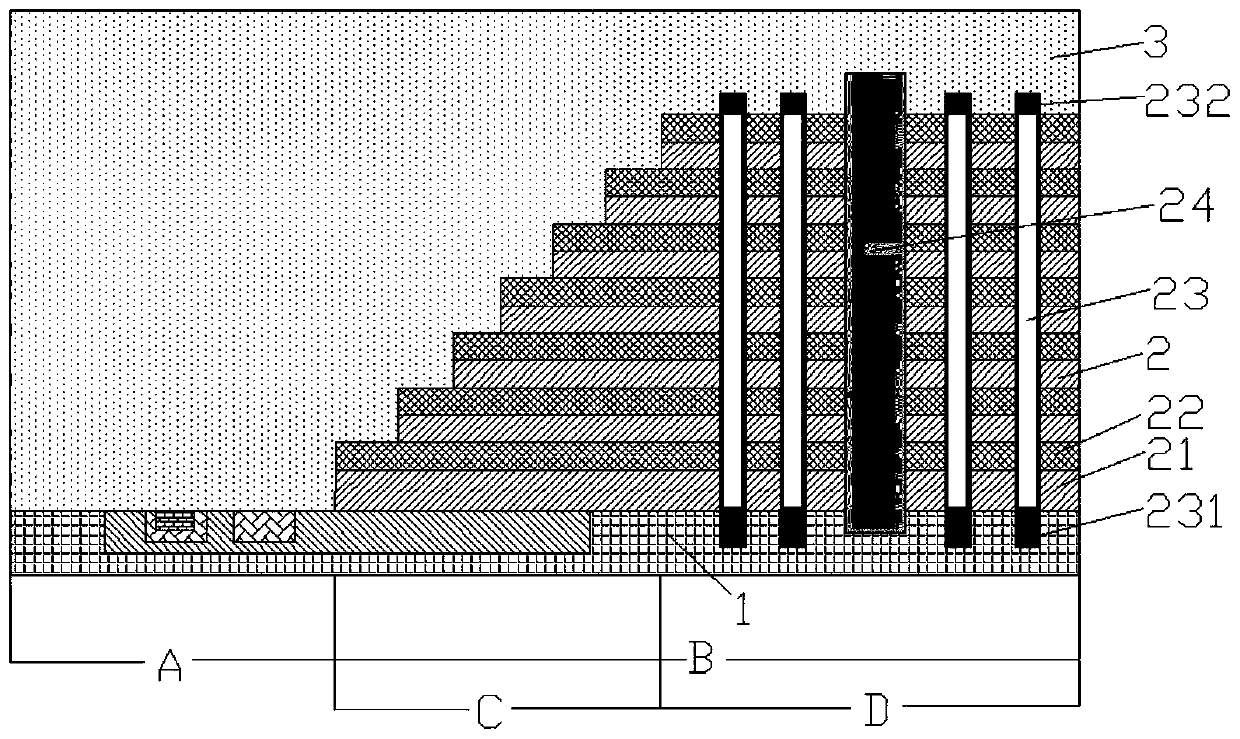
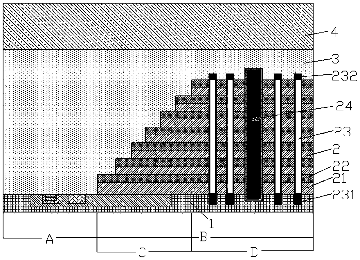
[0040] Traditional contacts and connectors are usually prepared separately. The following is a specific explanation: the preparation process of the contact is usually to deposit an interlayer dielectric layer on the surface of the flat layer of the semiconductor device, and then prepare a contact hole, then deposit a conductive material in the contact hole to form the contact, and finally remove the interlayer The deposited layer on the surface of the dielectric layer. The preparation process of the connector is usually to deposit an interlayer dielectric layer on the surface of the flat layer o...


PUM


Abstract

The invention provides a three-dimensional memory preparation method, which comprises the following steps: providing a semiconductor device, wherein the semiconductor device comprises a substrate, a step structure and a flat layer, the step structure is arranged on the substrate and comprises a step part and a storage part, and the flat layer covers the substrate and the step structure; forming aninterbedding dielectric layer on the surface of the flat layer; forming a plurality of contact holes and a plurality of through holes which penetrate through the interbedding dielectric layer and theflat layer, wherein the contact holes correspond to the substrate and/or the step part, and the through holes correspond to the storage part; providing a conductive material, forming a contact in thecontact hole and forming a connector in the through hole. The preparation method according to the invention integrates the producing processes of the contact and the connector, greatly reducing the time and cost for producing the contact and the connector as well as the time and cost for producing the three-dimensional memory. The invention also provides a three-dimensional memory and an electronic device.

Description

Technical field [0001] The invention belongs to the field of semiconductor technology, and specifically relates to a preparation method of a three-dimensional memory, a three-dimensional memory, and electronic equipment. Background technique [0002] As a storage device that is better than a hard disk drive, three-dimensional memory is also a non-volatile storage product with low power consumption, light weight, and excellent performance, and has been more and more widely used in electronic products. With the continuous development of three-dimensional memory, the composition and structure of the three-dimensional memory are becoming more and more complex. Therefore, it is bound to increase the process steps, increase the production cost and prolong the production cycle during the preparation, which will eventually lead to the reduction of corporate profits. [0003] The existing manufacturing process of the contact and the connection element will significantly increase the product...

Claims


Application Information

Patent Timeline
IPC IPC(8): H01L27/11526H01L27/11556H01L27/11573H01L27/11582H01L27/11531
CPCH10B41/42H10B41/40H10B43/40H10B41/27H10B43/27
Inventor 赵婷婷鲍琨夏志良宋豪杰吴建中刘磊张含玉
Owner YANGTZE MEMORY TECH CO LTD
Why Eureka
Try Eureka