OLED display device and fabrication method thereof

A display device and display area technology, which is applied in the manufacturing of semiconductor/solid-state devices, electric solid-state devices, semiconductor devices, etc., can solve the problem that the camera area cannot be displayed, and achieves the improvement of imaging effect, transmittance, and reduction of occlusion area. Effect

Active Publication Date: 2019-07-23
WUHAN CHINA STAR OPTOELECTRONICS SEMICON DISPLAY TECH CO LTD
View PDF5 Cites 14 Cited by
  • Summary
  • Abstract
  • Description
  • Claims
  • Application Information

AI Technical Summary

Problems solved by technology

[0009] An object of the present invention is to provide an OLED display device and its preparation method, which can solve the problem that the camera area of ​​the current OLED display device cannot display

Method used


Image

  • OLED display device and fabrication method thereof
  • OLED display device and fabrication method thereof
  • OLED display device and fabrication method thereof

Examples


Embodiment 1

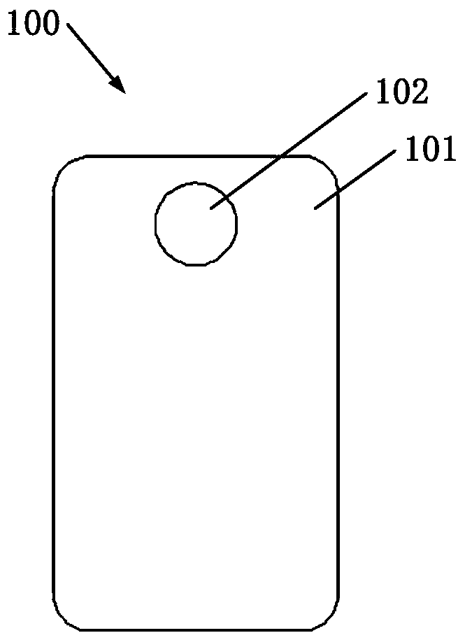
[0053] Such as figure 1 As shown, an OLED display device 100 is defined with a first display area 101 and a second display area 102 .

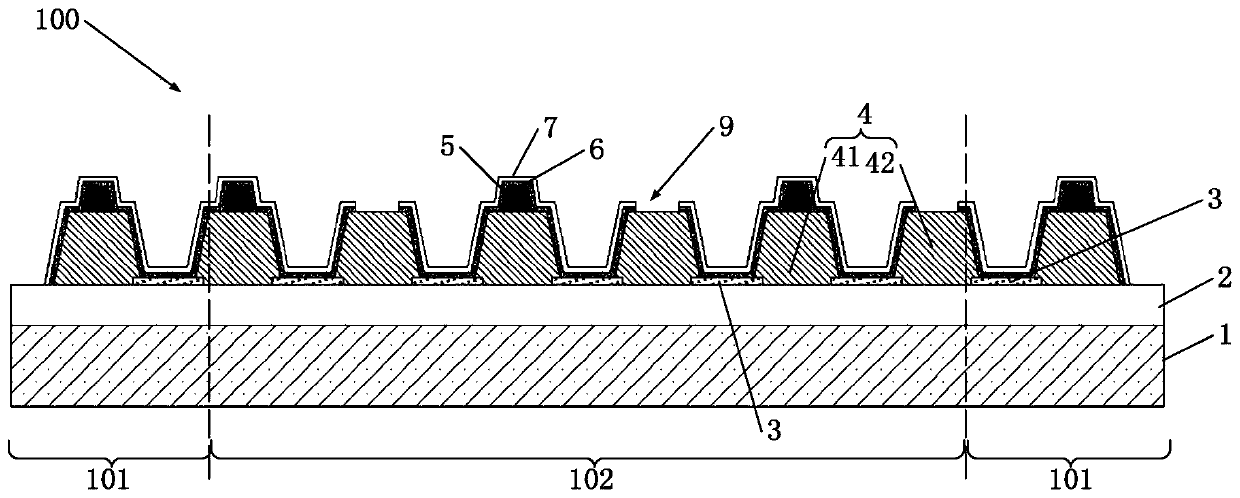
[0054] Such as figure 2 As shown, the OLED display device 100 shown therein comprises: a substrate 1 , a functional layer 2 , an anode 3 , a pixel definition layer 4 , a first isolation column 5 , a light emitting layer 6 and a cathode 7 . The functional layer 2 is disposed on the substrate 1 ; the anodes 3 are disposed on the functional layer 2 at intervals; the pixel definition layer 4 is disposed on the functional layer 2 between adjacent anodes 3 .

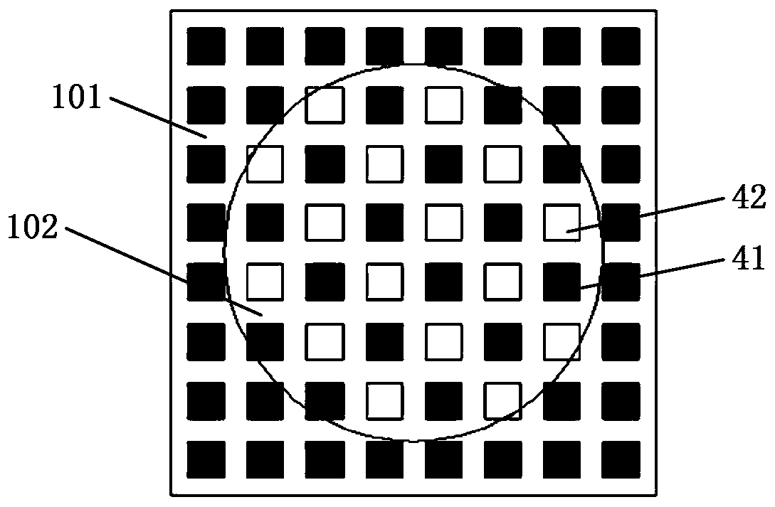
[0055] Such as figure 2 , image 3 As shown, the pixel definition layer 4 of the first display region 101 is provided with first isolation columns 5 . Wherein the pixel definition layer 4 located in the second display area 102 includes a first pixel definition layer 41 and a second pixel definition layer 42; the first isolation column 5 is arranged on the first pixel definition layer 41;...

Embodiment 2

[0059] In the following, only the differences between the present embodiment and the first embodiment will be described, and the similarities will not be repeated here.

[0060] Such as Figure 5 , Figure 6 As shown, there are two second pixel definition layers 42 arranged between the two adjacent first pixel definition layers 41. Thus, the shaded area of ​​the cathode 7 can be reduced, the transmittance of the cathode 7 can be increased, and finally the lighting effect of the camera under the screen can be improved, and the imaging effect thereof can be improved.

Embodiment 3

[0062] In the following, only the differences between the present embodiment and the first embodiment will be described, and the similarities will not be repeated here.

[0063] Such as Figure 7 , Figure 8 As shown, there are three or more second pixel definition layers arranged between two adjacent first pixel definition layers. Thus, the shaded area of ​​the cathode 7 can be reduced, the transmittance of the cathode 7 can be increased, and finally the lighting effect of the camera under the screen can be improved, and the imaging effect thereof can be improved.


PUM


Abstract

The invention relates to an OLED display device and a fabrication method thereof. The OLED display device comprises a substrate, a functional layer, a positive electrode, a pixel defining layer, a first isolation vertical post, a light emitting layer and a negative electrode. An upper surface of the negative electrode on a second pixel defining layer is locally sunken until a groove is formed in abottom surface of the light emitting layer, so that the shielding area of the negative electrode is reduced, the transmittance of the negative electrode is improved, the lighting effect of a camera under a screen is finally improved, and the imaging effect is improved.

Description

technical field [0001] The invention relates to the field of display technology, in particular to an OLED display device and a preparation method thereof. Background technique [0002] OLED (full name in English: Organic Light-Emitting Diode, Organic Light-Emitting Diode) display device is also called organic electro-laser display device, organic light-emitting semiconductor. [0003] The basic structure of an OLED is a sandwich structure, usually consisting of an anode, a luminescent material, and a cathode wrapped into a sandwich-like structure. The whole structural layer includes: hole transport layer (HTL), light emitting layer (EL) and electron transport layer (ETL). When the power is supplied to an appropriate voltage, positive holes and surface cathode charges will combine in the light-emitting layer, and under the action of Coulomb force, they will recombine with a certain probability to form excitons (electron-hole pairs) in an excited state, and this The excited ...

Claims


Application Information

Patent Timeline
Patent Type & Authority Applications(China)
IPC IPC(8): H01L51/50H01L51/52H01L51/56H01L27/32
CPCH10K59/122H10K50/00H10K50/82H10K50/84H10K71/00H10K59/121
Inventor 张明杨杰
Owner WUHAN CHINA STAR OPTOELECTRONICS SEMICON DISPLAY TECH CO LTD
Why Eureka
Try Eureka