LED display screen driving chip and latch signal generation method and system
A LED display and driver chip technology, applied to static indicators, instruments, etc., can solve the problem of occupying a lot of port resources, and achieve the effect of simplifying the structure and reducing the number of external ports
- Summary
- Abstract
- Description
- Claims
- Application Information
AI Technical Summary
Problems solved by technology
Method used
Image

Examples
Embodiment 1
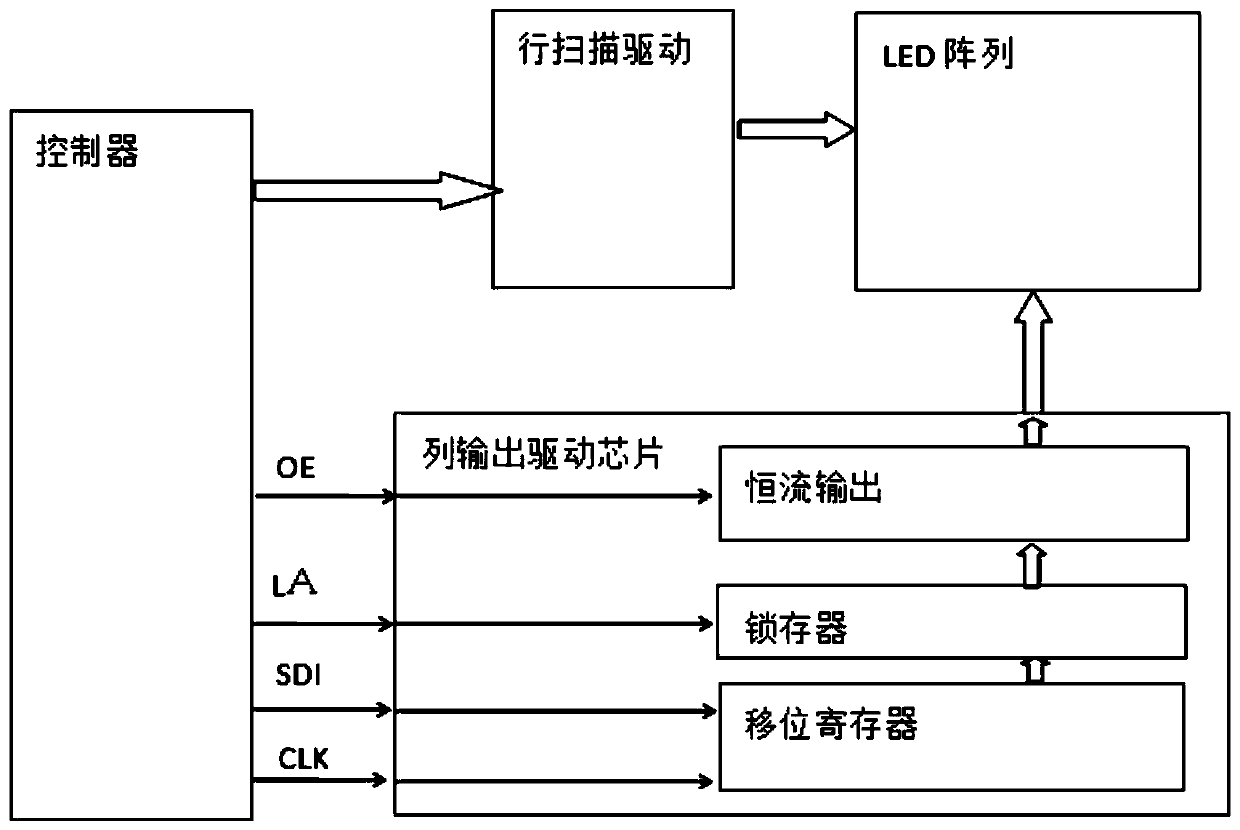
[0047] A kind of LED display driver chip, see figure 2, including a controller, a row scanning drive unit, an LED array, and a column output drive unit; wherein the output of the controller is connected to the input of the row scan drive unit, and the output of the row scan drive unit is connected to the LED array;
[0048] The column output driving unit includes a shift register, a latch and a constant current output unit; the data output port (hereinafter referred to as the SDI port) and the clock port (hereinafter referred to as the CLK port) of the controller are connected to the shift register, and the shift register The output end of the bit register is connected to the input end of the latch, the output end of the latch is connected to the input end of the constant current output unit, and the output end of the constant current output unit is connected to the LED array; the use of the controller The energy port is connected to the control terminal of the constant curre...
Embodiment 2
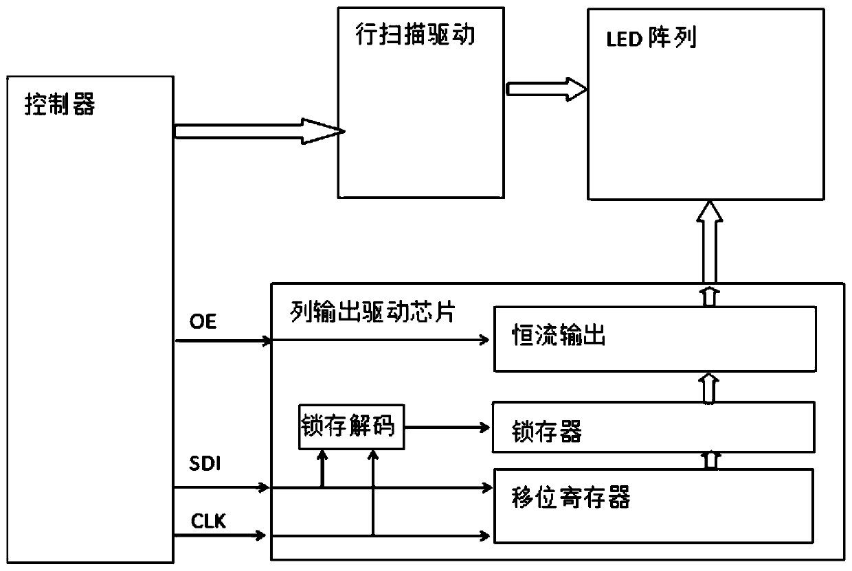
[0057] Embodiment two adds the following content on the basis of embodiment one:
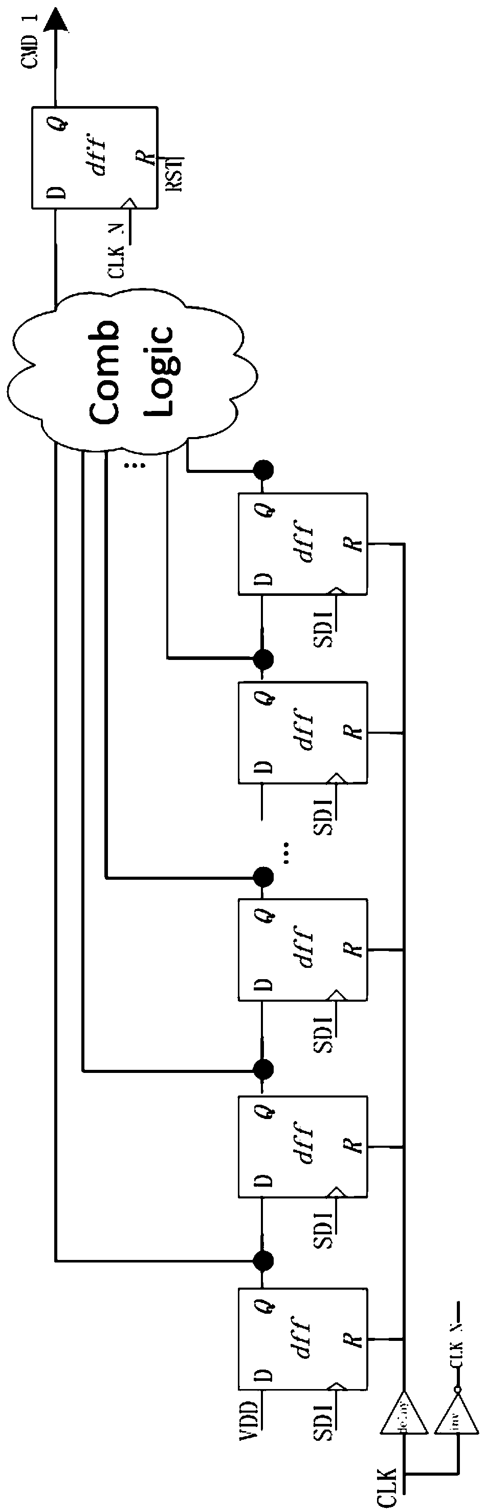
[0058] see image 3 In the figure, both the first D flip-flop and the second D flip-flop are represented by dff, the delay unit is represented by delay, the inverter is represented by inv, and the combinational logic unit is represented by comb logic.
[0059] The latch decoding unit includes a plurality of first D flip-flops, a delay unit, an inverter, a combinational logic unit, and a second D flip-flop;
[0060] All the first D flip-flops are connected in series, wherein the power supply terminal of the first D flip-flop is connected to the positive power supply, and the power supply terminal of the N+1 first D flip-flop is connected to the output terminal of the N-th first D flip-flop ; The output terminals of all the first D flip-flops are connected to the input terminals of the combinational logic unit; the data segments of all the first D flip-flops are connected to the data output port ...
Embodiment 3
[0067] A kind of latch signal generation method of LED display driver chip, see Figure 4 , including the following steps:
[0068] S1: When the rising edge of the clock port output of the controller is detected, the timer is started;
[0069] S2: When it is detected that the clock port of the controller is at a high level and the data output port outputs a pulse, the timer is incremented by 1;
[0070] S3: When the clock port of the controller is detected to output a falling edge, stop the timer timing;
[0071] S4: Read the data of the timer. When the data of the timer is greater than or equal to the preset latch threshold, a latch signal is generated and output to the latch.
[0072] specifically, Figure 5 For the existing 4-wire control mode. The SDI data is shifted into the shift register at the rising edge of the CLK signal, and then the data in the shift register is locked to the latch at the high level of the LA signal.
[0073] Figure 6 The 3-wire control mode...
PUM
 Abstract
Description
Claims
Application Information
 - R&D
- Intellectual Property
- Life Sciences
- Materials
- Tech Scout
- Unparalleled Data Quality
- Higher Quality Content
- 60% Fewer Hallucinations
Browse by: Latest US Patents, China's latest patents, Technical Efficacy Thesaurus, Application Domain, Technology Topic, Popular Technical Reports.
© 2025 PatSnap. All rights reserved.Legal|Privacy policy|Modern Slavery Act Transparency Statement|Sitemap|About US| Contact US: help@patsnap.com