Circuit board structure and manufacturing method thereof

A manufacturing method and circuit board technology, which is applied to printed circuits, printed circuits, printed circuits assembled with electrical components, etc., can solve problems such as multiple costs, lower yields, and complicated manufacturing, and achieve reduced manufacturing costs and high process requirements. , the effect of simplifying the process

Active Publication Date: 2021-08-10
UNIMICRON TECH CORP
View PDF0 Cites 0 Cited by
  • Summary
  • Abstract
  • Description
  • Claims
  • Application Information

AI Technical Summary

Problems solved by technology

In this way, the production is more complicated and requires more cost, and may lead to a decrease in yield (yield)

Method used


Image

  • Circuit board structure and manufacturing method thereof
  • Circuit board structure and manufacturing method thereof
  • Circuit board structure and manufacturing method thereof

Examples


Embodiment Construction

[0063] The foregoing and other technical content, characteristics and efficacy of the present invention will be clearly presented in detail below with reference to the various embodiments of the drawings. The direction used in the following examples, such as "upper", "lower", "front", "post", "left", "right", etc., is only the direction of the additional drawings. Therefore, the direction term used is illustrated, and is not intended to limit the invention. Also, in the following examples, the same or similar components will use the same or similar reference numerals.

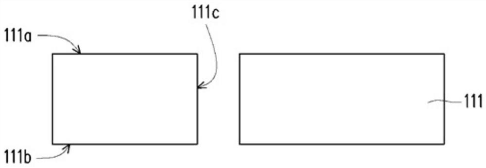
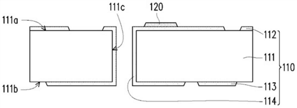
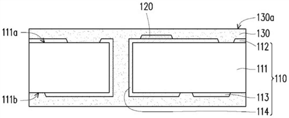
[0064] Figures 1A to 1G It is a cross-sectional view of a manufacturing process of a circuit board structure according to an embodiment of the present invention. Figure 1h Yes Figure 1G The enlarged view of the middle region R. Figure 1I Yes Figure 1G The upper view schematic of the middle region r. For the sake of clarity, Figure 1I In the middle, a portion of the die or component is omitted.

[0065] The method ...


PUM


Abstract

The invention provides a circuit board structure and a manufacturing method thereof. The circuit board structure includes an insulating layer, a first circuit layer and a second circuit layer on opposite sides of the insulating layer, and the insulating layer is penetrated to electrically connect the first circuit layer and the second circuit layer. Conductive vias, capacitor dielectric layers, dielectric layers and redistributed circuit layers of the circuit layer. The first wiring layer includes a first capacitor electrode. The capacitive dielectric layer is located on the first capacitive electrode. The dielectric layer covers the first circuit layer and the capacitor dielectric layer. The redistributed circuit layer includes a redistributed circuit on the dielectric layer, a first conductive blind hole located in the dielectric layer and connected to the first circuit layer, and a second capacitor electrode located in the dielectric layer. Two ends of the second capacitor electrode are respectively in contact with the capacitor dielectric layer and the redistribution line. The second capacitor electrode, the capacitor dielectric layer and the first capacitor electrode constitute a capacitor.

Description

Technical field [0001] The present invention relates to a circuit board structure and a method thereof, in particular, to a circuit board structure having a capacitor and a method of fabricating it. Background technique [0002] With the demand of electronic products, the stronger the function of the function of the signal transmission is high speed and circuit components, and the number of passive components that is combined with the consumer electronics is also increased. Furthermore, in the electronics emphasize the light and short, how to accommodate the large number of electronic components in a limited consolidation space, which has become an electronic confession, an eunuch, a technology bottleneck, and overcoming technology. In order to solve this problem, the configuration technique gradually went to the system integration phase of the SMS IN Package; SIP, especially the package of multi-chipmodule; MCM. Among them, inner bury active components and passive components tec...

Claims


Application Information

Patent Timeline
Patent Type & Authority Patents(China)
IPC IPC(8): H05K1/18H05K3/32
CPCH05K1/185H05K3/32H05K2201/10015
Inventor 谢育忠陈裕华简俊贤
Owner UNIMICRON TECH CORP
Why Eureka
Try Eureka