Image sensor and forming method thereof

An image sensor and graphics technology, applied in the direction of electric solid-state devices, semiconductor devices, electrical components, etc., can solve the problem of low sensitivity of photodiodes, and achieve the effect of good image and high sensitivity

Active Publication Date: 2019-08-16
HUAIAN IMAGING DEVICE MFGR CORP
View PDF5 Cites 0 Cited by
  • Summary
  • Abstract
  • Description
  • Claims
  • Application Information

AI Technical Summary

Problems solved by technology

[0005] The technical problem to be solved by the technical solution of the present i

Method used


Image

  • Image sensor and forming method thereof
  • Image sensor and forming method thereof
  • Image sensor and forming method thereof

Examples


Example Embodiment

[0023] At present, when the image sensor is working, the incident light is first filtered into three monochromatic lights of red, blue and green through a filter, and then the corresponding photodiodes collect the corresponding optical signals, output electrical signals, and restore the image through difference calculation. . Since the photodiode only has the function of photoelectric conversion, in the case of weak light, the light sensitivity is not enough, which affects the imaging effect of the image sensor.

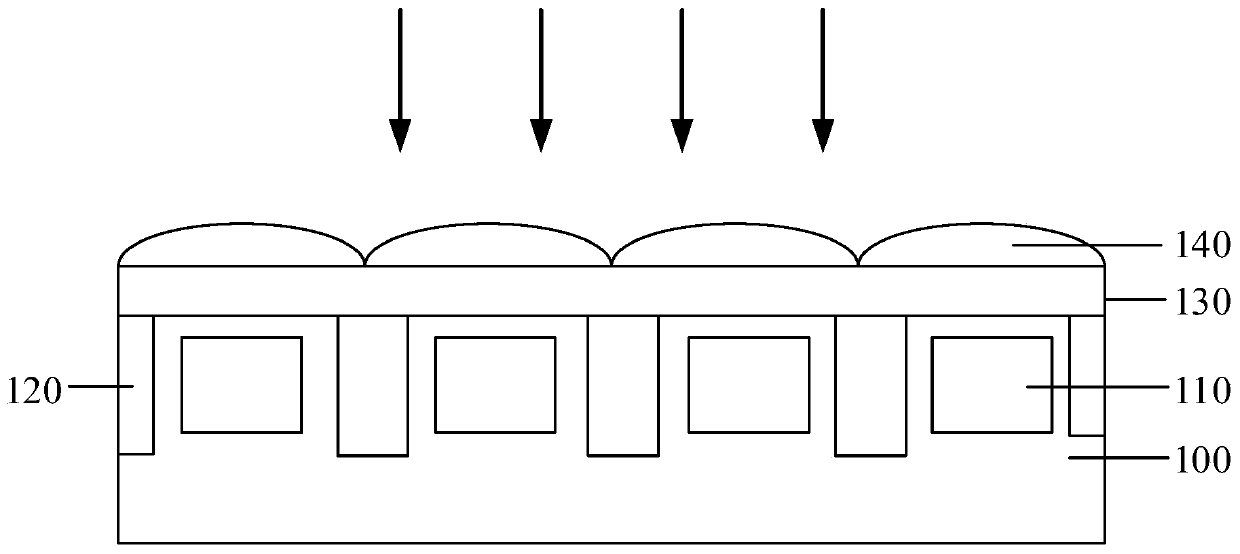
[0024] figure 1 is a structural schematic diagram corresponding to the formation process of the image sensor. refer to figure 1 , providing a semiconductor substrate 100, in which discrete photodiodes 110 are formed, and the discrete photodiodes 110 are isolated by deep trench isolation structures 120, and the depth of the deep trench isolation structures 120 is Deeper than the photodiode 110, so as to obtain a better isolation effect and avoid the problem of phot...


PUM


Abstract

The technical scheme of the invention discloses an image sensor and a forming method thereof. The forming method includes the following steps: a first substrate is provided, wherein the first substrate has a first surface and a second surface, and the first surface and the second surface are opposite to each other; discrete photoelectric transistors are formed in the first substrate; and filter layers are formed on the first surface, wherein each filter layer corresponds to one photoelectric transistor. The optical signal is enhanced, and the sensitivity is improved.

Description

technical field [0001] The invention relates to the technical field of semiconductor manufacturing, in particular to an image sensor and a forming method thereof. Background technique [0002] An image sensor is a device that converts an optical image into an electrical signal. With the development of the computer and communication industries, the demand for high-performance image sensors is increasing. These high-performance image sensors are widely used in digital cameras, video recorders, personal communication systems (PCS), game consoles, security cameras, and medical miniature cameras. various fields. [0003] Image sensors are generally of two types, Charge Coupled Device (CCD) sensors and CMOS Image Sensors (CMOS Image Sensors, CIS). Compared with CCD image sensors, CMOS image sensors have the advantages of high integration, low power consumption, and low production cost. Traditional image sensors, whether they are CMOS image sensors or CCD image sensors, use phot...

Claims


Application Information

Patent Timeline
IPC IPC(8): H01L27/146
CPCH01L27/14621H01L27/14681H01L27/14685
Inventor 刘亮亮陈伯廷吴宗祐林宗贤
Owner HUAIAN IMAGING DEVICE MFGR CORP
Why Eureka
Try Eureka