Check patentability & draft patents in minutes with Patsnap Eureka AI!

Pixel compensation circuit and OLED display device

A technology of compensation circuit and display device, applied in static indicators, instruments, etc., to achieve the effect of compressing size and realizing high PPI panel design

Active Publication Date: 2019-08-23
WUHAN CHINA STAR OPTOELECTRONICS SEMICON DISPLAY TECH CO LTD
View PDF7 Cites 4 Cited by
  • Summary
  • Abstract
  • Description
  • Claims
  • Application Information

AI Technical Summary

Problems solved by technology

That is, due to the layout of the components in the pixel compensation circuits such as 7T1C, 6T1C, and 6T2C, the size of the pixel structure is limited to be further reduced, which in turn limits the improvement of the pixel density (Pixels Per Inch, PPI for short).

Method used


Image

  • Pixel compensation circuit and OLED display device
  • Pixel compensation circuit and OLED display device
  • Pixel compensation circuit and OLED display device

Examples


Embodiment Construction

[0019] Embodiments of the present invention are described in detail below, examples of which are shown in the drawings, wherein the same or similar reference numerals denote the same or similar components or components having the same or similar functions throughout. The embodiments described below by referring to the figures are exemplary only for explaining the present invention and should not be construed as limiting the present invention. Furthermore, the present disclosure repeats reference numerals and / or reference letters in different examples, such repetition is for the purpose of simplicity and clarity and does not in itself indicate a relationship between the various embodiments and / or arrangements discussed.

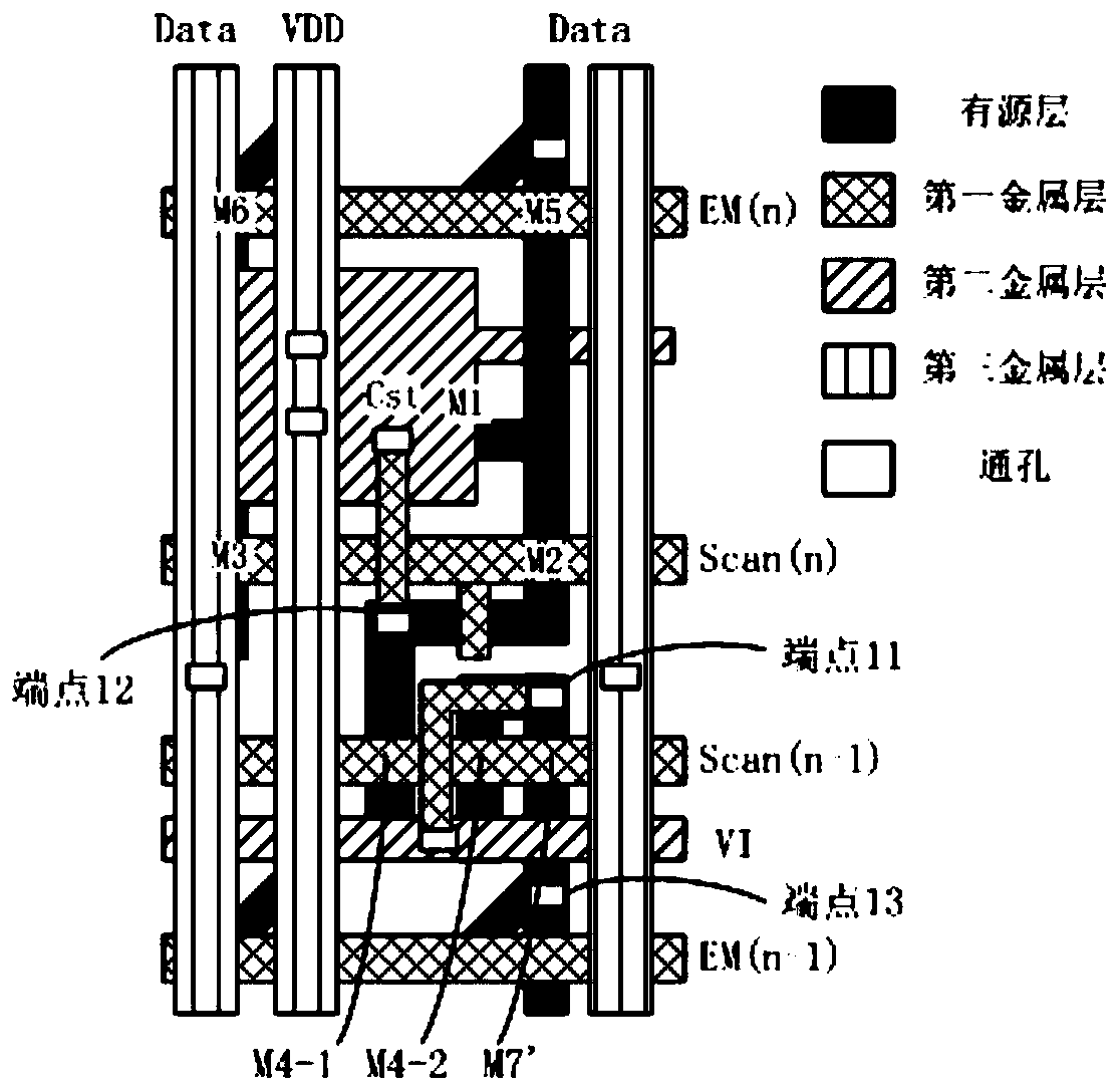
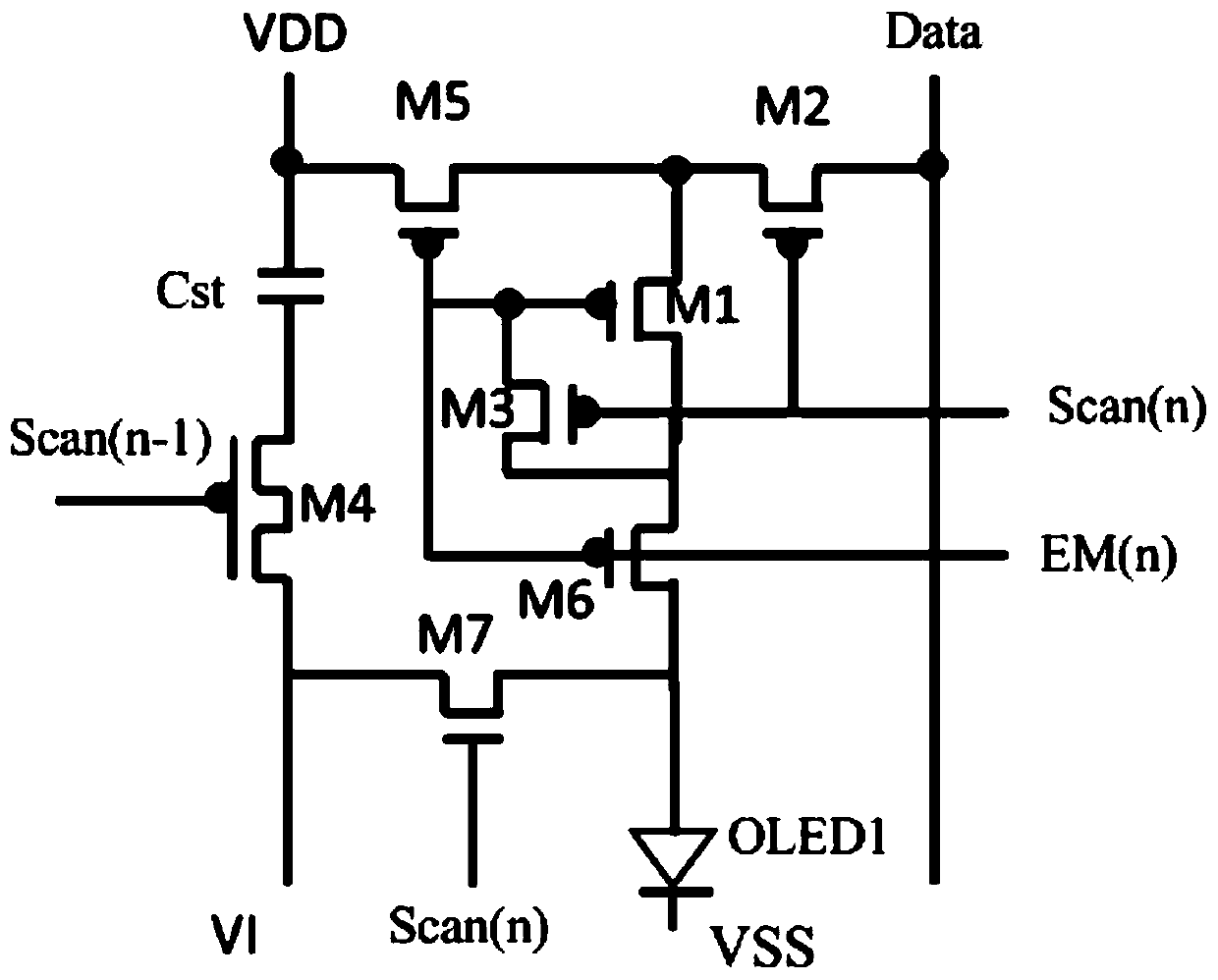
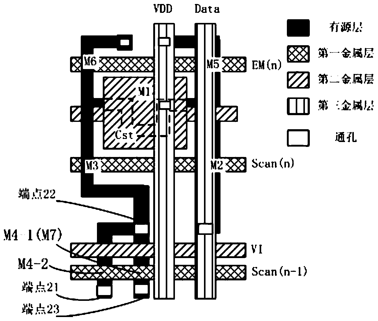
[0020] The pixel compensation circuit of the present invention is applied to a pixel structure, the pixel structure includes a reset voltage signal line and a plurality of scanning signal lines, and the pixel compensation circuit includes a fourth transistor an...


PUM


Abstract

The invention discloses a pixel compensation circuit and an OLED display device. At least two thin film transistors are controlled by scanning signals output by the same row of scanning signal lines,so that an organic light emitting diode and a storage capacitor are both communicated with a reset voltage signal line, and the reset voltage signal is received by the organic light emitting diode andthe storage capacitor to be reset. According to at least two thin film transistors controlled by the same row of scanning signals, the polycrystalline silicon wires of the active layer can be only two wires in the vertical direction, so that the size of the pixel structure in the horizontal direction can be compressed, space is provided for improvement of PPI, and the design of the high PPI panelis facilitated.

Description

technical field [0001] The invention relates to the field of display technology, in particular to a pixel compensation circuit and an OLED display device. Background technique [0002] In recent years, the rapid development of OLED (Organic Light Emitting Diode, Organic Light Emitting Diode) display technology has promoted the rapid entry of curved surface and flexible display products into the market, and technological updates in related fields are also changing with each passing day. OLED refers to a diode that uses organic semiconductor materials and light-emitting materials to cause light emission through carrier injection and recombination under the drive of an electric field. Due to the advantages of light weight, self-luminescence, wide viewing angle, low driving voltage, high luminous efficiency, low power consumption, and fast response speed, OLED display devices are widely used. In an OLED pixel circuit, the OLED in the pixel circuit can be driven to emit light th...

Claims


Application Information

Patent Timeline
Patent Type & Authority Applications(China)
IPC IPC(8): G09G3/3266G09G3/3225
CPCG09G3/3266G09G3/3225G09G3/3233
Inventor 王威徐品全
Owner WUHAN CHINA STAR OPTOELECTRONICS SEMICON DISPLAY TECH CO LTD
Features
  • R&D
  • Intellectual Property
  • Life Sciences
  • Materials
  • Tech Scout
  • Unparalleled Data Quality
  • Higher Quality Content
  • 60% Fewer Hallucinations
Learn More