Strong microcavity silicon-based organic light-emitting display device and forming method thereof

A technology of light-emitting display and organic light-emitting layer, which is applied in the direction of electrical components, electric solid devices, circuits, etc., can solve the problems of weak micro-cavity effect, large electrode height drop, and difficult control of depth accuracy, so as to reduce uneven optical scattering , precise thickness control, and improved display effect

Active Publication Date: 2019-08-23
SEEYA OPTRONICS LTD
View PDF4 Cites 7 Cited by
  • Summary
  • Abstract
  • Description
  • Claims
  • Application Information

AI Technical Summary

Problems solved by technology
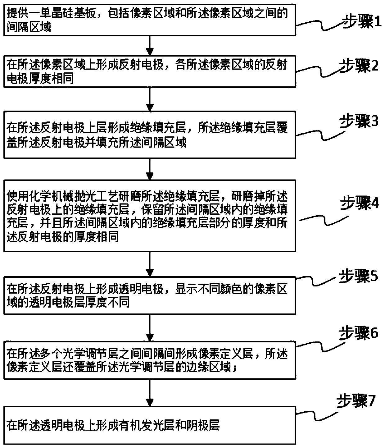
However, it is difficult to achieve different groove depths only by adjusting the exposure capability and exposure time, and the depth accuracy is difficult to control. The microcavity effect is weak and it is difficult to form a strong microcavity effect.
However, if the reflective electrodes and transparent electrode layers of different heights are directly fabricated on the insulating layer without passing through the trenches, the problem is that the height difference between the electrodes between different pixels is too large, which leads to the problem that the cathode is easy to break.
Furthermore, the height difference between the reflective electrode and the transparent electrode is large, which brings another problem that the pixel definition layer is difficult to make flat. When light passes through the uneven pixel definition layer, diffuse reflection will occur, resulting in a halo phenomenon. reduced contrast

Method used


Image

  • Strong microcavity silicon-based organic light-emitting display device and forming method thereof
  • Strong microcavity silicon-based organic light-emitting display device and forming method thereof
  • Strong microcavity silicon-based organic light-emitting display device and forming method thereof

Examples


Embodiment 1

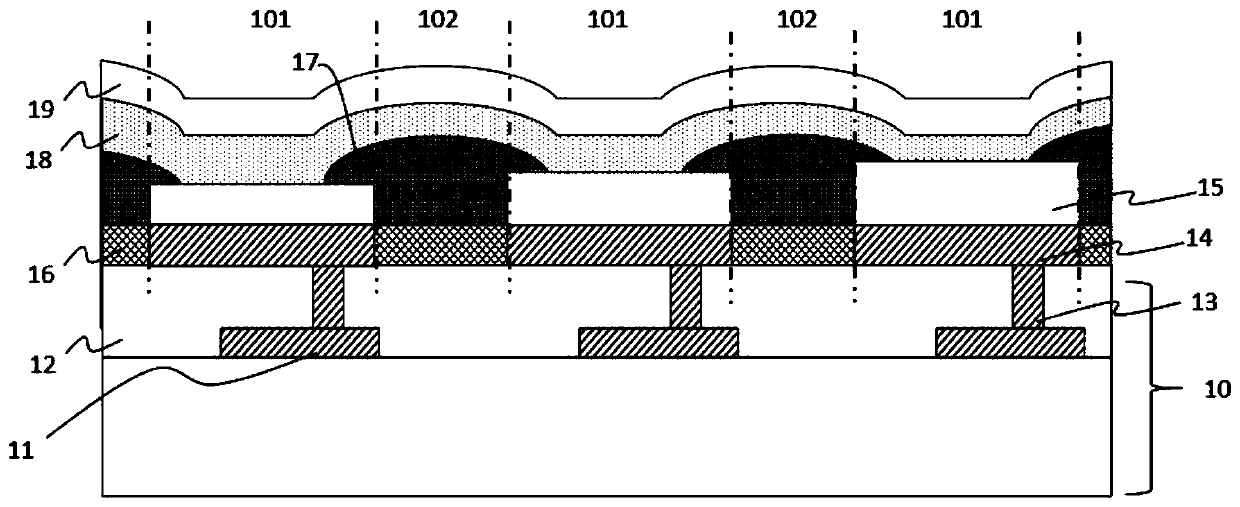
[0038] Please refer to figure 2 , figure 2 A schematic diagram of a strong microcavity silicon-based organic light-emitting display device provided for Embodiment 1 of the present invention, as shown in the figure, includes: a single crystal silicon substrate 10, on which the single crystal silicon substrate 10 includes a driving circuit layer, and the driving circuit layer includes pixels The driving structure 11 such as the driving circuit, the gate driving circuit, and the source driving circuit is provided with an insulating layer 12 on the upper layer of the driving structure 11 . A through hole 13 is provided in the insulating layer 12 to transmit the signal of the pixel driving circuit to the reflective electrode 14 .

[0039] The single crystal silicon substrate 10 includes pixel regions 101 and spacer regions 102 disposed between the pixel regions 101 , the reflective electrodes 14 are disposed in the pixel regions 101 , and the reflective electrodes 14 of each pix...

Embodiment 2

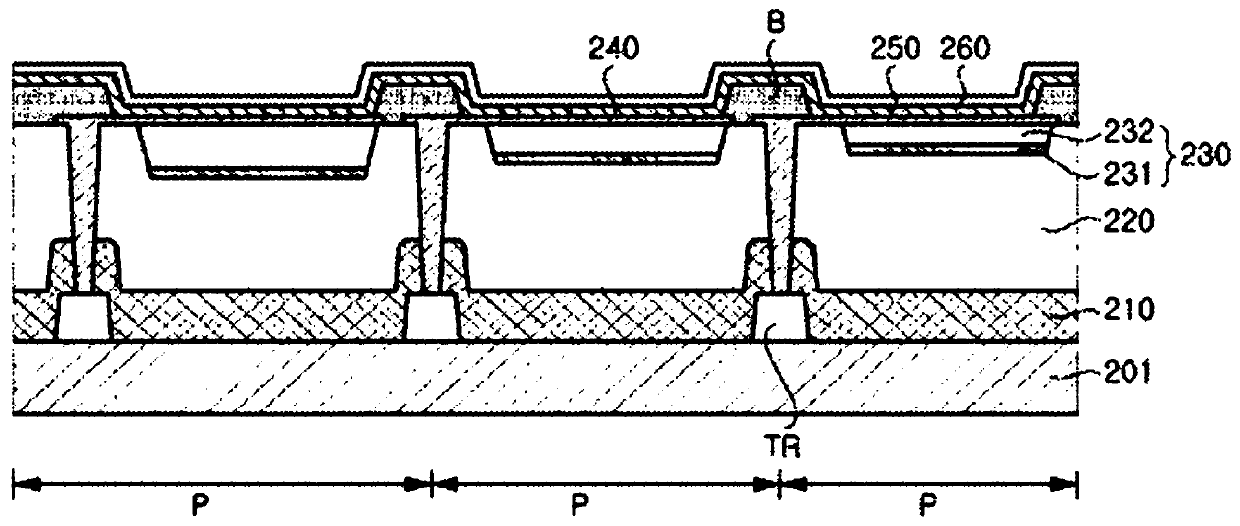
[0060] Please refer to Figure 7 , Figure 7 A schematic diagram of a strong microcavity silicon-based organic light-emitting display device provided for Embodiment 2 of the present invention, as shown in the figure, includes: a single crystal silicon substrate 20, and the single crystal silicon substrate 20 includes a driving circuit layer, and the driving circuit layer includes pixels The driving structure 21 such as the driving circuit, the gate driving circuit, and the source driving circuit is provided with an insulating layer 22 on the upper layer of the driving structure 21 . A through hole 23 is provided in the insulating layer 22 to transmit the signal of the pixel driving circuit to the reflective electrode 24 .

[0061] The single crystal silicon substrate 20 includes pixel regions 201 and spacer regions 202 arranged between the pixel regions 201, the reflective electrodes 24 are arranged in the pixel regions 201, and the reflective electrodes 24 of the pixel regio...


PUM


Abstract

The invention provides a strong micro-cavity silicon-based organic light-emitting display device, which comprises a monocrystalline silicon substrate. The monocrystalline silicon substrate comprises pixel regions and interval regions between the pixel regions. Reflecting electrodes are arranged in the pixel regions, and transparent electrodes are arranged on the reflecting electrodes. An insulation filling layer is arranged in the interval regions. A pixel definition layer is arranged on the insulation filling layer. The pixel definition layer further covers the edges of the transparent electrodes. An organic light-emitting layer is arranged on the pixel definition layer. A cathode layer is arranged on the organic light-emitting layer. The invention further provides a forming method of thestrong micro-cavity silicon-based organic light-emitting display device. According to the strong micro-cavity silicon-based organic light-emitting display device and the forming method thereof, the difference in the film forming time period of the pixel definition layer is reduced or eliminated, and the breakage is avoided. The thickness is uniform. The halo phenomenon caused by optical scattering unevenness caused by partial unevenness of the pixel definition layer on the edge of the transparent electrode is further reduced. The contrast ratio of the display device is improved.

Description

technical field [0001] The invention relates to the display field, in particular to a strong microcavity silicon-based organic light-emitting display device and a forming method thereof. Background technique [0002] Organic light-emitting display devices, ie, Organic Light-Emitting Diode (OLED) display devices, have been favored by industry insiders because of their thinness, power saving and many other incomparable advantages compared to liquid crystal display devices. The OLED display device is different from the traditional liquid crystal display device in that it does not need a backlight. It uses a very thin organic material coating on the substrate. When an electric current passes through, these organic materials will emit light. Moreover, the OLED display device can be made lighter and thinner, has a larger viewing angle, and can significantly save power. [0003] Among the technologies for enhancing brightness, there is a microcavity technology. A microcavity repr...

Claims


Application Information

Patent Timeline
Patent Type & Authority Applications(China)
IPC IPC(8): H01L27/32H01L51/52H01L51/56
CPCH10K59/35H10K59/122H10K50/805H10K50/856H10K71/00
Inventor 曾章和钱栋李启沈永财
Owner SEEYA OPTRONICS LTD
Why Eureka
Try Eureka