A kind of gallium nitride semiconductor photoelectrochemical etching solution and processing method
A photoelectrochemical, etching solution technology, applied in chemical instruments and methods, semiconductor/solid-state device manufacturing, circuits, etc., can solve problems such as inability to achieve etching speed, affect the performance of GaN-based devices, and avoid boundary effects. Effect
- Summary
- Abstract
- Description
- Claims
- Application Information
AI Technical Summary
Problems solved by technology
Method used
Image

Examples
Embodiment 1
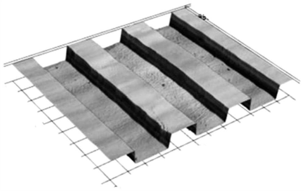
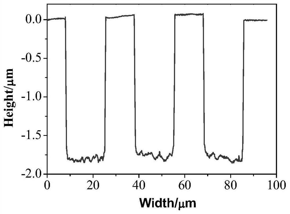
[0029] figure 1 and figure 2 The gallium nitride surface groove structure ( figure 1 ) and its cross-sectional view ( figure 2 ).
[0030] Preparation and use method: use pure water to make etching solution (pH=3), its composition includes 10mM potassium hydrogen persulfate compound salt (K 2 SO 4 ·KHSO 4 ·2KHSO 5 ), 0.5mM phosphoric acid and phosphate buffer; the gallium nitride wafer that has been deposited on the surface with a metal platinum gate layer (thickness=100nm) is immersed in the above-mentioned etching solution; 2 After the gallium nitride wafer was irradiated with light intensity for one hour, it was taken out and washed with pure water; after the etched wafer was immersed in 20% (by weight) hydrofluoric acid solution for 10 minutes, it was taken out, washed with pure water, and dried.
[0031] The photoelectrochemically etched GaN wafer surface was characterized by optical method (LSM). figure 1 It is the groove structure on the surface of gallium nit...
Embodiment 2
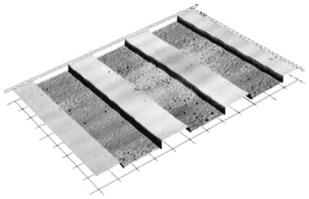
[0033] image 3 and Figure 4 The gallium nitride surface groove structure ( image 3 ) and its cross-sectional view ( Figure 4 ).
[0034] Preparation and use method: use pure water to make etching solution (pH=6.5), its composition includes 5mM potassium hydrogen persulfate compound salt (K 2 SO 4 ·KHSO 4 ·2KHSO 5 ), 5mM phosphoric acid and phosphate buffer; the gallium nitride wafer with a layer of metal platinum gate layer (thickness=100nm) deposited on the surface is immersed in the above-mentioned etching solution; 2 After the gallium nitride wafer was irradiated with light intensity for 45 minutes, it was taken out and washed with pure water; after the etched wafer was immersed in 20% (by weight) hydrofluoric acid solution for 10 minutes, it was taken out, washed with pure water, and dried.
[0035] Optical methods were used to characterize the surface of GaN wafer after photoelectrochemical etching. image 3 It adopts the groove structure on the surface of gal...
Embodiment 3
[0037] Figure 5 and Figure 6 The gallium nitride surface groove structure ( Figure 5 ) and its cross-sectional view ( Figure 6 ).
[0038] Preparation and use method: adopt pure water to make etching solution (pH=2), its composition includes 40mM potassium hydrogen persulfate compound salt (K 2 SO4·KHSO 4 ·2KHSO 5 ) and 2mM phosphoric acid and phosphate buffer; the gallium nitride wafer with one deck metal platinum gate layer (thickness=100nm) deposited on the surface is immersed in the above-mentioned etching solution; 2 After irradiating the gallium nitride wafer with light intensity for half an hour, take it out, and wash it with pure water; after immersing the etched wafer in 20% (by weight) hydrofluoric acid solution for 10 minutes, take it out, wash it with pure water, and blow dry.
[0039] Optical methods were used to characterize the surface of GaN wafer after photoelectrochemical etching. Figure 5It adopts the groove structure on the surface of gallium ni...
PUM
| Property | Measurement | Unit |
|---|---|---|
| thickness | aaaaa | aaaaa |
Abstract
Description
Claims
Application Information
 - R&D
- Intellectual Property
- Life Sciences
- Materials
- Tech Scout
- Unparalleled Data Quality
- Higher Quality Content
- 60% Fewer Hallucinations
Browse by: Latest US Patents, China's latest patents, Technical Efficacy Thesaurus, Application Domain, Technology Topic, Popular Technical Reports.
© 2025 PatSnap. All rights reserved.Legal|Privacy policy|Modern Slavery Act Transparency Statement|Sitemap|About US| Contact US: help@patsnap.com