Adjusting system and method for preventing probe mark from deviating in wafer test

A wafer testing and adjustment system technology, applied in electronic circuit testing, electrical measurement, and measurement devices, etc., can solve problems such as human judgment differences, reduce machine utilization, and fail to find test problems in time, and achieve the effect of ensuring test quality.

Inactive Publication Date: 2019-08-30
HUAIAN IMAGING DEVICE MFGR CORP
View PDF25 Cites 4 Cited by
  • Summary
  • Abstract
  • Description
  • Claims
  • Application Information

AI Technical Summary

Problems solved by technology

[0003] The current practice is to conduct manual needle mark inspection before the test, there are differences in human judgment, and subsequent test problems cannot be found in time
In addition, the level of the carrier table where the wafer is placed is often adjusted manually by adding gaskets and locking screws, which reduces the utilization rate of the machine and increases the tedious adjustment and calibration time.

Method used


Image

  • Adjusting system and method for preventing probe mark from deviating in wafer test
  • Adjusting system and method for preventing probe mark from deviating in wafer test
  • Adjusting system and method for preventing probe mark from deviating in wafer test

Examples


Embodiment Construction

[0029] The making and using of the embodiments are discussed in detail below. It should be understood, however, that the specific embodiments discussed are merely illustrative of specific ways to make and use the invention, and do not limit the scope of the invention. The expression of the structural position of each component such as up, down, top, bottom, etc. in the description is not absolute, but relative. These directional expressions are appropriate when the various components are arranged as shown in the drawings, but when the positions of the various components in the drawings are changed, these directional expressions are also changed accordingly.

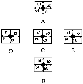
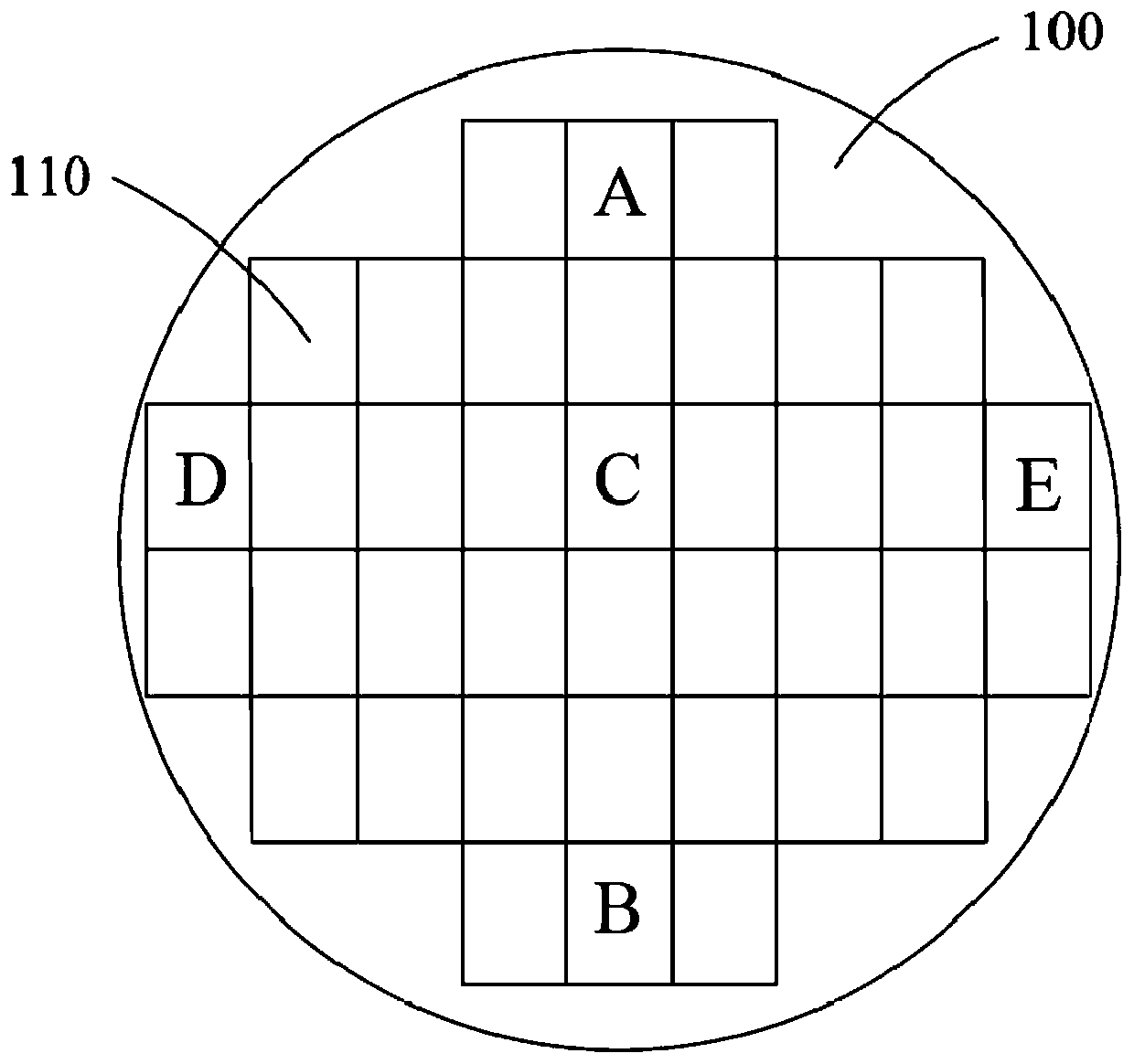
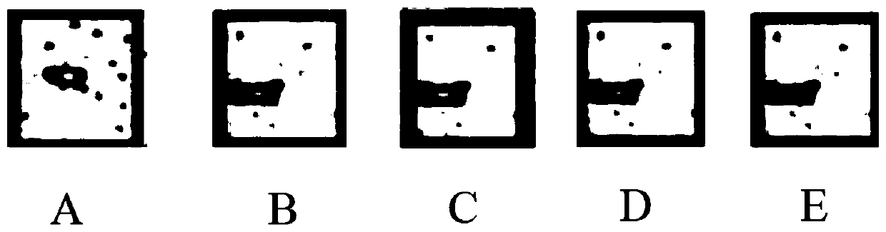
[0030] Wafer testing is aimed at the complete die on the entire chip, and the pads on each die are tested by means of probes, which are used to screen the good and bad products of the die on the chip. Wafer testing is to use the combination of testing machine, needle testing machine and probe card to test each die on the...


PUM


Abstract

The invention provides an adjusting system and method for preventing a probe mark from deviating in a wafer test. The adjusting system comprises: a probe tester comprising a bearing table used for adsorbing a wafer to be tested; a probe card comprising a probe used to be in contact with bonding pads on a plurality of crystal grains of the wafer, wherein probe marks are formed at the surfaces of the bonding pads; and a controller. The adjusting method comprises the steps of: adsorbing a wafer on a bearing table of a probe tester; selecting a plurality of crystal grains from the crystal grains of the wafer; allowing the probe of the probe card to be in contact with the bonding pads on the crystal grains, and forming probe marks at the surfaces of the bonding pads; inspecting the formed probemarks by the controller, determining whether the probe marks are deviated or not according to an inspection result, if yes, calculating the height compensation value of the crystal grains where the probe marks are located; and adjusting the levelness of the bearing table of the probe tester according to the height compensation value by the controller so as to prevent the probe marks from deviating in the wafer test.

Description

technical field [0001] The invention relates to the technical field of semiconductors, in particular to an adjustment system and an adjustment method for preventing needle mark deviation in wafer testing. Background technique [0002] With the pursuit of integrated circuit area cost and the need for special functional structures, CUP (circuit under pad, that is, placing circuits under the pad) structure design gradually appeared. The structural design is to place active devices such as MOS transistors (transistors with a Metal-Oxide-Semiconductor structure) under bond pads to save area. For this structure, due to the stress generated by needle sticking or bonding during the test, it is easy to cause the electrical parameters of the CUP to drift, which will lead to poor test stability. For CP (wafer test), in order to accurately measure the electrical parameters of MOS transistors, it is necessary to avoid unpredictable errors caused by the CUP structure. The most important ...

Claims


Application Information

Patent Timeline
IPC IPC(8): G01R31/28
CPCG01R31/2887
Inventor 周杰熊望明田茂
Owner HUAIAN IMAGING DEVICE MFGR CORP
Why Eureka
Try Eureka