Semiconductor device and operation method thereof

A semiconductor and equipment technology, applied in the field of semiconductor integrated circuit manufacturing, can solve the problems of increasing the risk of particle pollution, the risk of wafer falling and fragmentation, reducing the efficiency of wafer processing, and affecting product yield, so as to avoid particle pollution and the risk of fragmentation, The effect of reducing the wafer transfer process and improving product yield

Inactive Publication Date: 2019-09-03
HUAIAN IMAGING DEVICE MFGR CORP
View PDF4 Cites 4 Cited by
  • Summary
  • Abstract
  • Description
  • Claims
  • Application Information

AI Technical Summary

Problems solved by technology

[0004] However, for the quality control of wafer manufacturing, each additional step in the wafer transfer process is accompanied by an additional risk of particle contamination and the risk of wafer dropping and fragmentation
After completing the wet process on one side of the wafer, transferring it to the wafer flipping module for flipping requires an additional wafer transfer process, which will additionally increase the risk of particle contamination and the risk of wafer dropping and fragmentation, thereby affecting product yield
In addition, a single process chamber in existing equipment can only process the front or back side of the wafer, which also greatly reduces wafer processing efficiency and limits equipment throughput

Method used


Image

  • Semiconductor device and operation method thereof
  • Semiconductor device and operation method thereof
  • Semiconductor device and operation method thereof

Examples


Embodiment 1

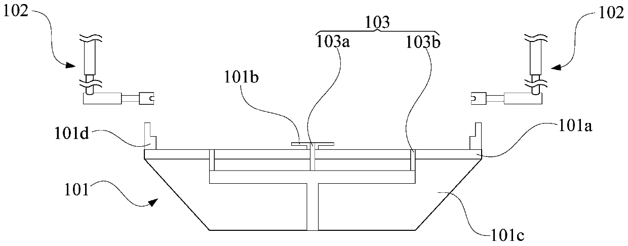
[0052] see Figures 1 to 5 , this embodiment provides a semiconductor device, including:

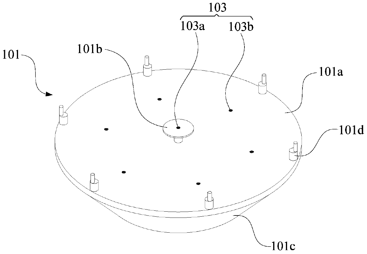
[0053] The wafer fixing platform 101 is used to fix the wafer during the process; the wafer fixing platform 101 is provided with a wafer placement position for accommodating the wafer at a specified position in a specified plane;

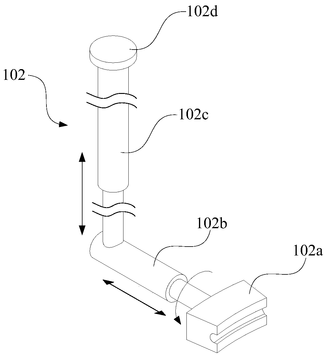
[0054] The wafer inverting device 102 is configured to invert the wafer relative to the specified plane.

[0055] Such as figure 1 Shown is a schematic cross-sectional view of the semiconductor device provided by this embodiment. Optionally, in this embodiment, the semiconductor equipment is a wet equipment used in a wafer wet process. exist figure 1Among them, the wafer fixing platform 101 is used to fix the wafer on the wafer placement position during the wet process, and the pair of wafer turning devices 102 are arranged on the wafer fixing platform 101 above. It should be pointed out that the semiconductor equipment is not limited to wet equipment, a...

Embodiment 2

[0063] see Figure 6 to Figure 12 , the present embodiment provides a method for operating a semiconductor device, comprising the following steps:

[0064] 1) Provide the semiconductor device as described in Embodiment 1 and the wafer 100 having opposite first surface and second surface;

[0065] 2) fixing the wafer 100 on the wafer placement position through the wafer fixing platform 101, the first surface and the second surface of the wafer 100 are respectively parallel to the designated plane;

[0066] 3) Flip the wafer 100 relative to the specified plane by the wafer inversion device 102, so that the first surface and the second surface of the wafer 100 are respectively parallel to the specified plane, and the The first surface faces the direction that the second surface before turning over faces, and the second surface faces the direction that the first surface before turning over faces.

[0067] In step 1), see Figure 6 S1 and figure 1 and Figure 7 , providing the...


PUM


Abstract

The invention provides a semiconductor device and an operation method thereof. The semiconductor device comprises: a wafer fixing platform used in a process to fix a wafer, wherein the wafer fixing platform is provided with a wafer placing position for accommodating the wafer at a specified position in a specified plane; and a wafer overturning device used for overturning the wafer relative to thespecified plane. According to the wafer overturning device, the wafer is overturned by introducing the wafer overturning device, so that the wafer conveying process additionally increased due to wafer overturning is reduced, the particulate pollution and the wafer breaking risk caused by the additionally increased wafer conveying process are avoided, and the product yield is improved.

Description

technical field [0001] The invention relates to the field of semiconductor integrated circuit manufacturing, in particular to a semiconductor device and an operation method. Background technique [0002] Wet processes such as wet etching or cleaning of wafers are important processes that affect the yield of semiconductor devices. With the continuous improvement of wet process requirements, monolithic wet process has been widely used in advanced manufacturing processes. In monolithic wet processing, a single process is performed only on the front or back side of the wafer. According to the requirements of the process, the wet process is also performed sequentially on the front and back of the wafer. [0003] Currently, in existing semiconductor equipment, separate process chambers are commonly used to perform wet processes on the front and back sides of the wafer respectively. During the wet process, the wafer is held front or back side up, and the upward surface of the wa...

Claims


Application Information

Patent Timeline
Patent Type & Authority Applications(China)
IPC IPC(8): H01L21/67
CPCH01L21/67051H01L21/6708
Inventor 云巴图陈章晏崔亚东颜超仁
Owner HUAIAN IMAGING DEVICE MFGR CORP
Why Eureka
Try Eureka