Electromagnetic wave shielding film, shielded printed wiring board, and electronic device

A technology for printed circuit boards and electronic equipment, applied in the fields of magnetic/electric field shielding, circuit devices, printed circuit components, etc., can solve the problems of interlayer tight bonding damage and poor shielding characteristics, and achieve high shielding characteristics, The effect of reducing the space and making the adhesion between layers difficult

Active Publication Date: 2019-09-03
TATSUTA ELECTRICWIRE & CABLE +1
View PDF5 Cites 0 Cited by
  • Summary
  • Abstract
  • Description
  • Claims
  • Application Information

AI Technical Summary

Problems solved by technology

Therefore, when rapid heating is performed in the solder reflow process, the volatile components accumulated between the shielding layer and the conductive adhesive layer

Method used


Image

  • Electromagnetic wave shielding film, shielded printed wiring board, and electronic device
  • Electromagnetic wave shielding film, shielded printed wiring board, and electronic device
  • Electromagnetic wave shielding film, shielded printed wiring board, and electronic device

Examples


Embodiment Construction

[0084] Hereinafter, the electromagnetic wave shielding film of this invention is demonstrated concretely. However, the present invention is not limited to the following embodiments, and can be appropriately modified and used without changing the gist of the present invention.

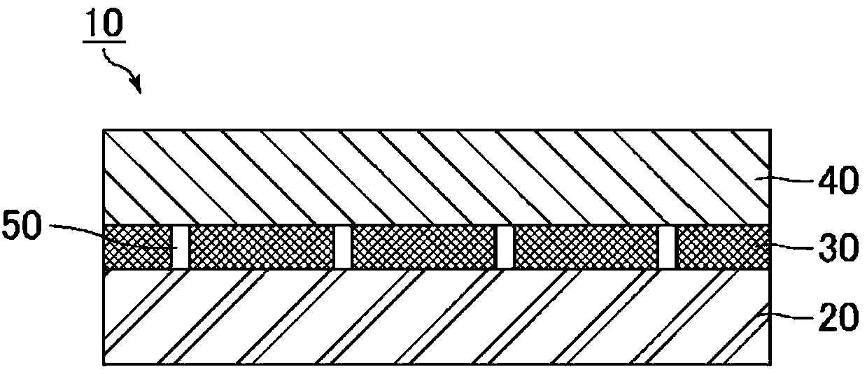
[0085] figure 2 It is a cross-sectional schematic diagram of an example of the electromagnetic wave shielding film of this invention.

[0086] Such as figure 2 As shown, the electromagnetic wave shielding film 10 includes a conductive adhesive layer 20 , a shielding layer 30 laminated on the conductive adhesive layer 20 , and an insulating layer 40 laminated on the shielding layer 30 .

[0087] In addition, a plurality of openings 50 are formed in the shield layer 30 .

[0088] (conductive adhesive layer)

[0089] In the electromagnetic wave shielding film 10 , the conductive adhesive layer 20 only needs to have conductivity and function as an adhesive, and may be made of any material.

[0090] F...


PUM

PropertyMeasurementUnit
Areaaaaaaaaaaa
Thicknessaaaaaaaaaa

Abstract

The purpose of the present invention is to provide an electromagnetic wave shielding film that has sufficient folding endurance and a sufficiently high electromagnetic wave shielding property. An electromagnetic wave shielding film according to the present invention comprises a conductive adhesive layer, a shielding layer that is laminated upon the conductive adhesive layer, and an insulating layer that is laminated upon the shielding layer. The electromagnetic wave shielding film is characterized in that a plurality of openings are formed in the shielding layer, no breaks occur when folded 600 times according to the MIT folding endurance test delimited in JIS P8115:2001, and the electromagnetic wave shielding property of the electromagnetic wave shielding film at 200 MHz as measured usingthe KEC technique is 85 dB or greater.

Description

technical field [0001] The invention relates to an electromagnetic wave shielding film, a shielding printed circuit board and electronic equipment. Background technique [0002] Conventionally, electromagnetic waves from the outside have been shielded by, for example, pasting an electromagnetic wave shielding film on a printed circuit board such as a flexible printed circuit board (FPC). [0003] An electromagnetic wave shielding film is generally formed by laminating a conductive adhesive layer, a shielding layer made of a metal thin film, etc., and an insulating layer in this order. The shielding printed circuit board is produced by hot pressing the electromagnetic wave shielding film and the printed circuit board in a state where the electromagnetic wave shielding film is bonded to the printed circuit board through an adhesive layer. After bonding, the components are mounted on the printed circuit board by solder reflow. In addition, the printed wiring board has a struc...

Claims


Application Information

Patent Timeline
IPC IPC(8): H05K9/00B32B3/18B32B7/025B32B15/08B32B15/20
CPCB32B3/18B32B7/02B32B15/08B32B15/20H05K9/00H05K9/0084H05K9/0088H05K1/0218
Inventor 上农宪治山内志朗白发润村川昭
Owner TATSUTA ELECTRICWIRE & CABLE
Why Eureka
Try Eureka