Method for reducing programming interference of 3d NAND memory

A programming interference and memory technology, applied in static memory, read-only memory, information storage, etc., can solve problems such as memory cell programming interference, and achieve the effect of reducing programming interference

Active Publication Date: 2021-05-18
YANGTZE MEMORY TECH CO LTD
View PDF7 Cites 0 Cited by
  • Summary
  • Abstract
  • Description
  • Claims
  • Application Information

AI Technical Summary

Problems solved by technology

[0004] In the prior art, when programming a certain memory cell in a certain channel hole, it is easy to cause programming interference to other memory cells in the same layer corresponding to other channel holes

Method used


Image

  • Method for reducing programming interference of 3d NAND memory
  • Method for reducing programming interference of 3d NAND memory
  • Method for reducing programming interference of 3d NAND memory

Examples


Embodiment Construction

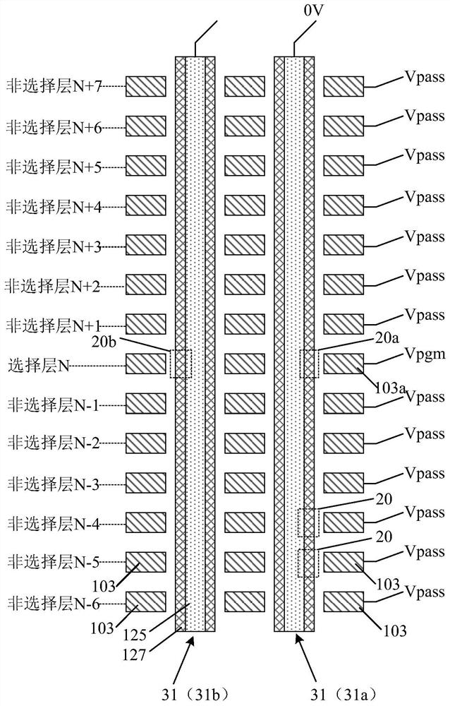
[0031] As mentioned in the background art, in the prior art, when programming a certain memory cell in a certain channel hole, it is easy to cause programming interference to other corresponding memory cells in the same layer in other channel holes.

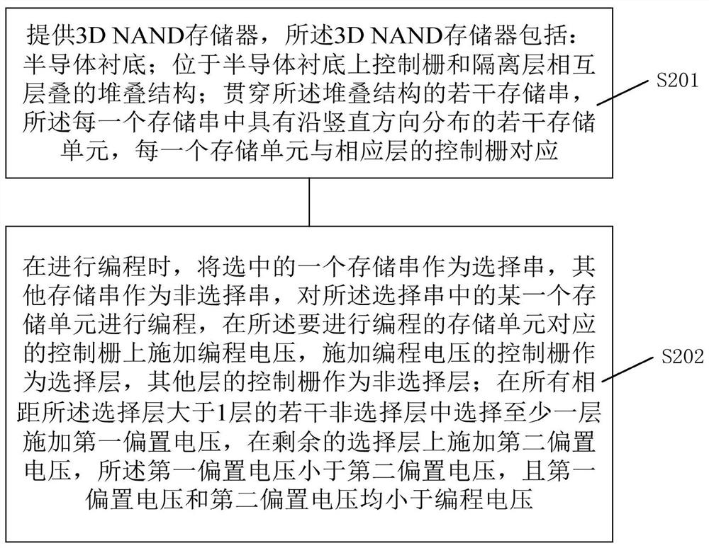
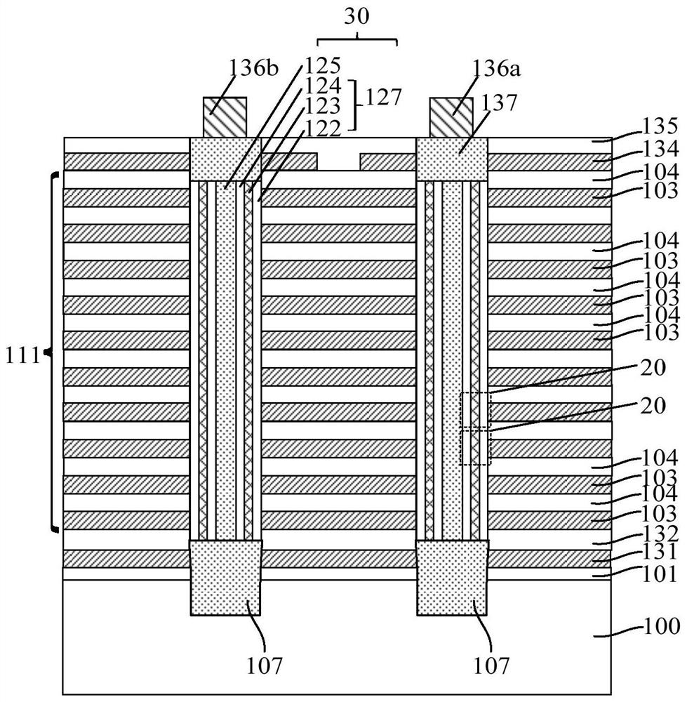
[0032]To this end, an embodiment of the present invention provides a 3D NAND memory programming method, including: providing a 3D NAND memory, refer to figure 1 , the 3D NAND memory includes: a semiconductor substrate; a stack structure in which the control gate 103 and the isolation layer are stacked on the semiconductor substrate; a number of storage strings 30 running through the stack structure, and each storage string 30 includes a channel Layer 125 and the storage layer 125 located on the sidewall of the channel layer, the position of the storage layer 125 corresponding to the control gate 103 of the corresponding layer is a storage unit 20, so that each storage string has several storage cells distributed along the vertical...


PUM


Abstract

A method for reducing programming interference of 3D NAND memory. When programming, a selected memory string is used as a selected string, and other memory strings are used as non-selected strings, and a certain memory cell in the selected string is programmed. Apply a programming voltage on the control gate corresponding to the memory cell to be programmed, use the control gate to which the programming voltage is applied as a selection layer, and control gates of other layers as a non-selection layer; A first bias voltage is applied to at least one of the non-selected layers, and a second bias voltage is applied to the remaining selected layers, the first bias voltage is smaller than the second bias voltage, and the first bias voltage and The second bias voltages are all lower than the programming voltage. The method of the present invention reduces the programming disturbance to the memory cell in the non-selected string which is located in the same layer as the programmed memory cell.

Description

technical field [0001] The invention relates to the field of semiconductor manufacturing, in particular to a method for reducing programming interference of 3D NAND memory. Background technique [0002] NAND flash memory is a better storage device than hard disk drives, and it has been widely used in electronic products as people pursue non-volatile storage products with low power consumption, light weight and high performance. At present, the planar NAND flash memory is close to the limit of practical expansion. In order to further increase the storage capacity and reduce the storage cost per bit, a 3D NAND memory is proposed. [0003] The existing 3D NAND memory structure includes: a semiconductor substrate; a stack structure in which a control gate and an isolation layer are stacked on the semiconductor substrate; several channel holes running through the stack structure; a storage structure located in the channel hole, the storage The structure includes a charge storage...

Claims


Application Information

Patent Timeline
Patent Type & Authority Patents(China)
IPC IPC(8): G11C16/34
CPCG11C16/3431
Inventor 王明刘红涛魏文喆李伟闵园园
Owner YANGTZE MEMORY TECH CO LTD
Why Eureka
Try Eureka