
Gate-enhanced light-controlled silicon-controlled-thyristor electrostatic release device structure and manufacturing method thereof

A technology of electrostatic discharge and device structure, applied in the direction of electric solid devices, electrical components, semiconductor devices, etc., can solve the problems that the internal core circuit cannot be effectively protected, the device's anti-ESD ability is insufficient, and the device's maintenance voltage is low. Improve the anti-ESD ability, strengthen the discharge ability, and reduce the effect of on-resistance

Active Publication Date: 2019-09-06
HUNAN NORMAL UNIVERSITY
View PDF10 Cites 0 Cited by
  • Summary
  • Abstract
  • Description
  • Claims
  • Application Information

AI Technical Summary

Problems solved by technology

However, since the triggering of traditional thyristors depends on the avalanche breakdown voltage of the reverse-biased PN junction on the trigger surface, the trigger voltage of this structure is relatively high
When the BJT is fully turned on, the maintenance voltage of the device is very low and cannot be adjusted, and it is easy to generate a latch inside the device, and when the traditional thyristor is used in a high-voltage environment, the ESD resistance of the device is also slightly insufficient
These defects will make the internal core circuit of the protected chip not effectively protected

Method used


Image

  • Gate-enhanced light-controlled silicon-controlled-thyristor electrostatic release device structure and manufacturing method thereof
  • Gate-enhanced light-controlled silicon-controlled-thyristor electrostatic release device structure and manufacturing method thereof
  • Gate-enhanced light-controlled silicon-controlled-thyristor electrostatic release device structure and manufacturing method thereof

Examples


Embodiment Construction

[0030] The present invention will be further described below in conjunction with the accompanying drawings and embodiments.

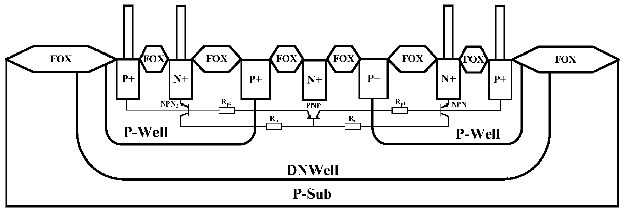
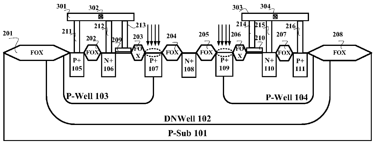
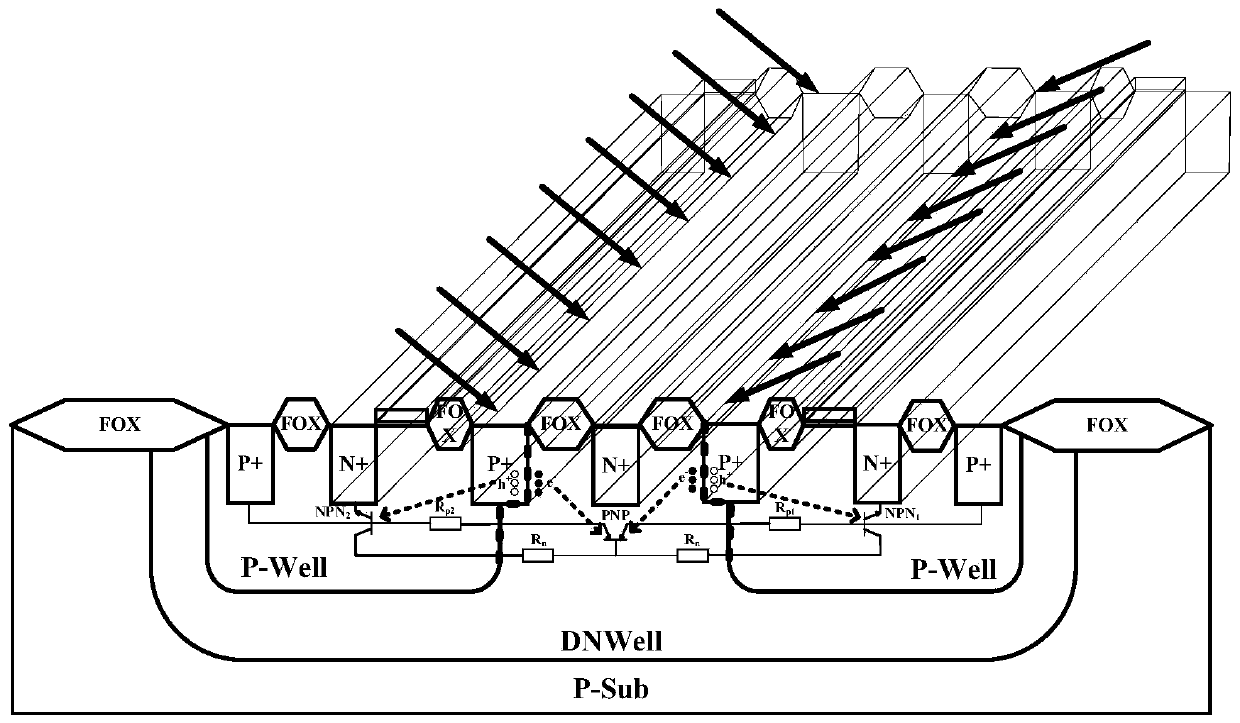
[0031] like Figure 1-Figure 6 As shown, a gate-enhanced phototriac electrostatic discharge device structure is characterized in that: it includes a substrate P-Sub101; the substrate P-Sub101 is provided with a DN-Well region 102; the DN-Well region The first P-Well region 103 and the second P-Well region 104 are sequentially arranged in 102 from left to right; the first field oxygen isolation region 201, The first P+ implantation region 105, the second field oxygen isolation region 202, the first N+ implantation region 106, the first polysilicon gate 209, the third field oxygen isolation region 203, and the second P+ implantation region 107; the second P The -Well region 104 is provided with the third P+ implantation region 109, the sixth field oxygen isolation region 206, the second polysilicon gate 210, the third N+ implantation region 110, the seve...


PUM


Abstract

The present invention discloses a gate-enhanced light-controlled silicon-controlled-thyristor electrostatic release device structure, including a substrate P-Sub. A DN-Well region is provided in the substrate P-Sub. A first P a Well zone and a second P-Well zone are provided in the DN-Well region. A first polysilicon gate and a second P+implant zone are provided in the first P-Well zone. A third P+implant zone and a second polysilicon gate are provided in the second P-Well zone. In the present invention, the first polysilicon gate, the second P+implant region, the third P+implant region, and the second polysilicon gate form a gate-enhanced light-controlled structure, so that a holding voltage of a two-way silicon controlled device can be adjustable. That is, photo-generated carriers generated by avalanche multiplication are used to adjust concentrations of P-Well and DN-Well, so that a concentration of a base region of a parasitic BJT changes, and an objective of changing emission efficiency and regulating and controlling the holding voltage is achieved.

Description

technical field [0001] The invention relates to the field of electrostatic protection, in particular to a structure of a grid-enhanced light-controlled thyristor electrostatic discharge device and a manufacturing method thereof. Background technique [0002] With the continuous progress of society and the continuous improvement of scientific level, the development of integrated circuits has entered the nanometer level. Electrostatic discharge (ESD) is one of the main causes of failure of integrated circuit chips, and the accumulation of static electricity is located in every aspect of human daily life. Therefore, more and more IC design engineers begin to pay attention to the protection of semiconductor ESD. According to relevant data, in the environment of integrated circuit and microelectronics, more than 58% of electronic products fail due to ESD phenomenon, and the resulting economic losses reach hundreds of billions. This data fully demonstrates the importance of elect...

Claims


Application Information

Patent Timeline
IPC IPC(8): H01L27/02
CPCH01L27/0262
Inventor 金湘亮汪洋
Owner HUNAN NORMAL UNIVERSITY
Learn More