Photonic crystal heterostructure capable of realizing broadband light wave one-way transmission

A technology of photonic crystals and heterostructures, applied in the direction of optical waveguide light guide, light guide, optics, etc., can solve the problems of relatively large fluctuations in forward transmission peaks and low one-way transmission bandwidth, and achieve easy preparation, simple structure, and high transmission rate effect

Active Publication Date: 2019-09-13
TAIYUAN UNIV OF TECH
View PDF7 Cites 7 Cited by
  • Summary
  • Abstract
  • Description
  • Claims
  • Application Information

AI Technical Summary

Problems solved by technology

Liu (L. Dan , S. Hu ,and Y. Gao . "One-way optical transmission in silicon photonic crystalheterojunction with circular and square scatterers." Physics LettersA(2017)), studied the orthogonal square air hole photonic crystal heterojunction Junction, although the one-way transmission bandwidth is about 0.04a/λ, but the fluctuation of the forward transmission peak is relatively large, and the forward high transmission cannot be maintained in a wide frequency range
[0004] Fei Hongming et al. (Fei Hongming, Xu Ting, Liu Xin, Lin Han, Chen Zhihui, Yang Yibiao, Zhang M

Method used


Image

  • Photonic crystal heterostructure capable of realizing broadband light wave one-way transmission
  • Photonic crystal heterostructure capable of realizing broadband light wave one-way transmission
  • Photonic crystal heterostructure capable of realizing broadband light wave one-way transmission

Examples


Embodiment Construction

[0021] In order to make the purpose, technical solutions and advantages of the embodiments of the present invention clearer, the technical solutions in the embodiments of the present invention will be clearly and completely described below. Obviously, the described embodiments are part of the embodiments of the present invention, rather than All the embodiments; based on the embodiments of the present invention, all other embodiments obtained by persons of ordinary skill in the art without creative work all belong to the protection scope of the present invention.

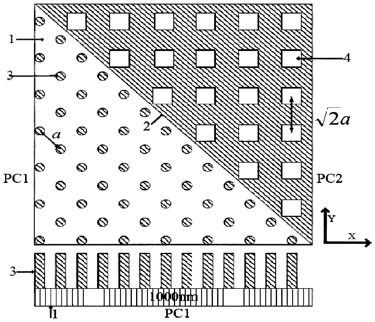
[0022] Such as figure 1 As shown, the embodiment of the present invention provides a photonic crystal heterostructure capable of realizing broadband light wave unidirectional transmission, including a silicon dioxide substrate 1 on which a thin silicon layer is grown; The silicon layer is bounded by the heterojunction interface 2, and a plurality of dielectric silicon cylinders 3 arranged periodically are etched on ...


PUM

PropertyMeasurementUnit
Thicknessaaaaaaaaaa
Thicknessaaaaaaaaaa
Radiusaaaaaaaaaa

Abstract

The invention belongs to the field of optical devices, and discloses a photonic crystal heterostructure capable of realizing broadband light wave one-way transmission. The photonic crystal heterostructure comprises a silicon dioxide substrate, on which is grown a thin silicon layer. By taking a heterojunction interface as a boundary, a plurality of medium silicon cylinders, which are periodicallyarranged are etched on the left side of the thin silicon layer, are used to form a first photonic crystal structure PC 1, and a plurality of square air holes, which are periodically arranged, are etched on the right side of the thin silicon layer to form a second photonic crystal structure PC 2. The height of the medium silicon cylinder and the depth of the square air holes are equal to the thickness of the thin silicon layer. The light wave is incident from the first photonic crystal structure PC 1 side, and is used to form an included angle of 45 degrees with the heterojunction interface. The photonic crystal heterostructure is easy to prepare, convenient to integrate, high in one-way transmittance, capable of realizing the one-way transmission characteristic of high forward transmissionand capable of being widely applied to the field of quantum optics.

Description

technical field [0001] The invention belongs to the field of optical devices, specifically to the field of optical quantum communication and quantum computing, and specifically relates to a photonic crystal heterogeneous structure capable of realizing broadband light wave unidirectional transmission. Background technique [0002] Unidirectional transmission of photonic diodes has become a key component of quantum computers due to their ability to perform logic operations. Due to the characteristics of small size, easy optical integration and low transmission loss, photonic crystals have become the preferred choice for the preparation of unidirectional transmission devices. Utilizing the energy band characteristics of photonic crystals, the photonic crystal structure can be designed to realize the one-way transmission of light waves, which has laid the foundation for the application of one-way transmission photonic diodes in quantum computing and information processing. [0...

Claims


Application Information

Patent Timeline
IPC IPC(8): G02B6/122G02B6/12
CPCG02B6/12G02B6/1225G02B2006/12038
Inventor 费宏明严帅武敏林翰杨毅彪张明达刘欣曹斌照陈智辉
Owner TAIYUAN UNIV OF TECH
Why Eureka
Try Eureka