Semiconductor device and forming method and working method thereof

A semiconductor and device technology, applied in the field of semiconductor devices and their formation, can solve problems such as performance to be improved, and achieve the effects of reducing the probability of particles, improving the yield, and reducing the probability

Inactive Publication Date: 2019-09-13
SEMICON MFG INT (SHANGHAI) CORP +1
View PDF7 Cites 0 Cited by
  • Summary
  • Abstract
  • Description
  • Claims
  • Application Information

AI Technical Summary

Problems solved by technology

[0004] However, the performance of semiconductor devices composed of f

Method used


Image

  • Semiconductor device and forming method and working method thereof
  • Semiconductor device and forming method and working method thereof
  • Semiconductor device and forming method and working method thereof

Examples


Example Embodiment

[0028] As mentioned in the background, semiconductor devices formed in the prior art have poor performance.

[0029] In order to make the above objects, features and beneficial effects of the present invention more comprehensible, specific embodiments of the present invention will be described in detail below in conjunction with the accompanying drawings.

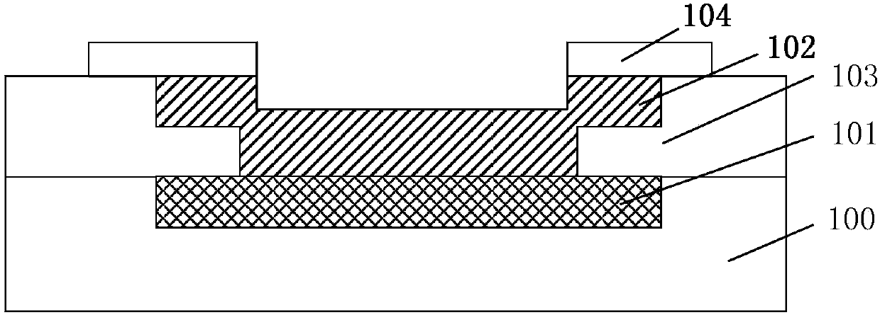
[0030] A semiconductor device, please refer to figure 1 , including: a semiconductor substrate 100; a device body (not shown) and pads located in the semiconductor substrate 100, the pads include a bottom pad layer 101, and a top pad layer 102, the bottom pad layer 101 and the top pad layer 102 The device body is electrically connected, and the top surface of the bottom pad layer 101 is flush with the top surface of the semiconductor substrate 100; the cover layer 103 on the bottom pad layer 101 has a top pad layer 102 in the cover layer, and the top pad layer 102 is located The surface of the bottom liner layer 101 ; the ...


PUM


Abstract

Disclosed are a semiconductor device and a forming method and a working method thereof; the semiconductor device comprises a semiconductor substrate, and a connecting gasket, a testing gasket and a wire located on the surface of the semiconductor substrate, wherein the semiconductor substrate comprises a device area and a non-device area; the semiconductor substrate device area is internally provided with a device main body and an interconnection structure which are electrically connected with each other; the connecting gasket is electrically connected with the testing gasket through the wire;the connecting gasket is located in the device area of the semiconductor substrate, and the testing gasket is located in the non-device area of the semiconductor substrate; and the wire is used for being fused after probe test is carried out, so that the connecting gasket and the testing gasket are disconnected. The performance of the semiconductor device is improved.

Description

technical field [0001] The invention relates to the field of semiconductor manufacturing, in particular to a semiconductor device and its forming method and working method. Background technique [0002] MOS (Metal-Oxide-Semiconductor) transistors are one of the most important components in modern integrated circuits. The basic structure of the MOS transistor includes: a semiconductor substrate; a gate structure located on the surface of the semiconductor substrate, and the gate structure includes: a gate dielectric layer located on the surface of the semiconductor substrate and a gate electrode layer located on the surface of the gate dielectric layer; The source and drain doped regions in the semiconductor substrate on both sides of the pole structure. [0003] With the development of semiconductor technology, the ability of the traditional planar MOS transistor to control the channel current becomes weaker, resulting in serious leakage current. Fin Field Effect Transisto...

Claims


Application Information

Patent Timeline
IPC IPC(8): H01L23/488H01L21/66
CPCH01L22/22H01L22/32H01L24/03H01L24/06H01L2224/06515
Inventor 熊鹏胡友存
Owner SEMICON MFG INT (SHANGHAI) CORP
Why Eureka
Try Eureka